That's right. As I said earlier measuring the resistance of the input is not of much use 🙂
Your problems seem to be centred around that zener diode. Check you know which way to put it in (they work as a zener one way and a normal diode the other), although it seems beyond use now so a new one is called for. I suspect you may have got it in the wrong way round and consequently it blew open circuit, which is why you have that much voltage across it.
Your problems seem to be centred around that zener diode. Check you know which way to put it in (they work as a zener one way and a normal diode the other), although it seems beyond use now so a new one is called for. I suspect you may have got it in the wrong way round and consequently it blew open circuit, which is why you have that much voltage across it.
It seems your zener is not a zener or is one with >Vrail breakdown voltage. The circuit begaves as if there was no zener connected. In this case, you get at best 1Vbe less bias voltaghe for the output stage which will not be enough to bias it over some few mA if that.
You can test the theory by connecting about 470-680 ohm resistor in parallel with 10nF or more capacitor (up to 10uF sill still be fine) instead of the zener. Your amp should alow proper idle current adjustment if all else is well, and it should work reasonably well too 😉
Before you do this, remember to turn the bias pot back to the minimum bias position!!!
i replaced the zener, it was a signal diode that i had incorrectly inserted when i replaced all the semi-conductors  (ilimzn was right!)
i now get 3.12V across it.
there is 5.6k ohm between ground and B of Q8 (ie 5.6K resistor is good)
Q8(NPN) on 'diode measurement' (out of circuit) =
red lead on E = nothing at C or B
blk lead on E = nothing at C and 804 at B
blk lead on C = nothing at E and 797 at B
red lead on B = 796 at C and 804 at E
Q9(NPN) on 'diode measurement' (out of circuit) =
red lead on E = nothing at C or B
blk lead on E = nothing at C and 808 at B
blk lead on C = nothing at E and 805 at B
red lead on B = 804 at C and 804 at E
ie they are good?
with Black lead on ground
vr1 @ 2 ohm
Q9
b=-0.26V
c=-0.19V
e=-0.40V
vr1 @ 186ohm (max)
Q9
b=-0.12V
c=-0.05V
e=-0.53V
(VR1 is working fine too)
------------
update on voltage across 'safety resistors': it seems there is a "fluctuating" voltage of about +/- 0.01V
so i set to AC and it is a solid ~0.005V on both sides (dunno if this is too small to be relevent?)
ALSO - the negative supply rail reaches 0V much faster than the positive supply rail - does this indicate anything?
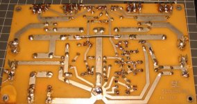
boholm - i have checked EVERY solder joint and actually re-soldered each joint to ensure that there are no soldering faults. i used my 50W halogen lamp to inspect the board very closely... there are no solder bridges...
also – I am measuring 0.25V at the Base of each output transistor and 0.025V at the Emitter of each output transistor...
still it draws no current!?!??!?!?!
*sigh*
any more wisdom from you gifted guys who are doing so well at trouble shooting an live electrical circut over the internet???
a very BIG thanks so far, if not for ALL your assistances, i certainly would have thought about giving up...
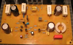
PS - here is a better picture of the circuit board - using MACRO on the digi-camera - sorry boholm!!!
(ilimzn was right!)i now get 3.12V across it.
there is 5.6k ohm between ground and B of Q8 (ie 5.6K resistor is good)
Q8(NPN) on 'diode measurement' (out of circuit) =
red lead on E = nothing at C or B
blk lead on E = nothing at C and 804 at B
blk lead on C = nothing at E and 797 at B
red lead on B = 796 at C and 804 at E
Q9(NPN) on 'diode measurement' (out of circuit) =
red lead on E = nothing at C or B
blk lead on E = nothing at C and 808 at B
blk lead on C = nothing at E and 805 at B
red lead on B = 804 at C and 804 at E
ie they are good?
ilimzn said:Please measure the voltages at B, C, E of Q9 with the bias pot first in one then the other extreme.
with Black lead on ground
vr1 @ 2 ohm
Q9
b=-0.26V
c=-0.19V
e=-0.40V
vr1 @ 186ohm (max)
Q9
b=-0.12V
c=-0.05V
e=-0.53V
(VR1 is working fine too)
------------
update on voltage across 'safety resistors': it seems there is a "fluctuating" voltage of about +/- 0.01V
so i set to AC and it is a solid ~0.005V on both sides (dunno if this is too small to be relevent?)
ALSO - the negative supply rail reaches 0V much faster than the positive supply rail - does this indicate anything?
boholm - i have checked EVERY solder joint and actually re-soldered each joint to ensure that there are no soldering faults. i used my 50W halogen lamp to inspect the board very closely... there are no solder bridges...
also – I am measuring 0.25V at the Base of each output transistor and 0.025V at the Emitter of each output transistor...
still it draws no current!?!??!?!?!
*sigh*
any more wisdom from you gifted guys who are doing so well at trouble shooting an live electrical circut over the internet???
a very BIG thanks so far, if not for ALL your assistances, i certainly would have thought about giving up...
PS - here is a better picture of the circuit board - using MACRO on the digi-camera - sorry boholm!!!
Attachments

Well, there is running current in the VAS stage now - just not enough, it seems.
With the new zener diode you *only* get 3.12 volts? You should be getting a bit more - around 3.3 - 3.4 volts. This could cause a limitation of current in the VAS stage, because the CE voltage of Q7 gets too small.
At Q7 - the 68 ohm resistor - is that now measuring the 0.9 volts?
Please also measure the voltage between C and E of Q9 with VR1 in both min. and max. You should get some voltage at max. - just not enough to turn on the output stage at this time.
tinkerbell said:i replaced the zener, it was a signal diode that i had incorrectly inserted when i replaced all the semi-conductors
i now get 3.12V across it.
there is 5.6k ohm between ground and B of Q8 (ie 5.6K resistor is good)
3.12 seems a bit low but if both Q7 and 8 are OK you may just have a high tolerance Zener. The slightly lower voltage will not make any great difference to the circuit function.
Another poster mentioned it influencing the current of the VAS stage (Q7, 8, 9) but this is wrong - it just sets bias for Q8, which is a cascode transistor for Q7. The voltage will be fine as long as it's between 3-5V, VAS current is set by the resistor in the emitter of Q9.
Per your measurements, Q8 and Q9 seem fine.
also – I am measuring 0.25V at the Base of each output transistor and 0.025V at the Emitter of each output transistor...
still it draws no current!?!??!?!?!
To check idle current you need to measure voltage between emitters of the output transistors. The actual offset at the output is not important at this time since you have no load (and do not connect any until the idle current problem is solved!).
Like another poster said, it seems you have either of two problems:
1) VAS current low - ckeck voltages on E and B of Q6
2) Output stage problem overloading Vbe multiplier Q9. To test this you can for starters measure the resistance across C/E of Q9 with the power off and everything in circuit, then we will see from there.
Please report what you have found and I'll see what other steps need to be taken...
Hm, one more thing: I may be stating the obvious but the board you photographed has no fuses for the output stage, hopefully you are measuring with these inserted 😉
Also, uppon looking carefully at your PCB, check that the insulation of the wire jumper has not breached and is not touching either E or C of Q9 (those are the two tracks closest to the solder joints for the jumper wire). If there is a connection, it is possible to get readings similar to yours.
I would advise that you put the wire on top. If you want to use a thicker one, you can drill the holes slightly larger, but it really won't matter - this wire is effectively in series with the emitter resistors of the output transistors, and it's resistance is only about 0.005 ohms, not much of a difference from the equivalent 0.235 of both emitter resistances. Also, the feedback is taken after it so it will compensate any resistance anyway.
If you wish to use a thicker wire for jumpers, i would advise you do so with the ground jumpers (two shorter ones just above the long output jumper), the resistance of these is more crytical. Even so, it is negligible compared to the PCB tracks so you should really not need to worry about that.
Finally, when adjusting idle current, if you need to keep the amp on for any length of time longer than a few seconds, the heatsink MUST be fitted otherwise there will be no thermal connection between output transistors and Q9, which is there to thermally compensate them so that thermal runaway does not happen (and thermal runaway = smoke out of output transistors!!!).
When testing are you using the 560R resistors across the fuse holders with no fuses in place and are you measuring voltage across these resistors.
I'd get rid of that link on the underside of the board and put it on top as can touch the ground or other tracks.
Not related to your problem, any reason why the fuse clips are on the underside of the PCB?
I'd get rid of that link on the underside of the board and put it on top as can touch the ground or other tracks.
Not related to your problem, any reason why the fuse clips are on the underside of the PCB?
boholm said:Well, there is running current in the VAS stage now - just not enough, it seems.
With the new zener diode you *only* get 3.12 volts? You should be getting a bit more - around 3.3 - 3.4 volts. This could cause a limitation of current in the VAS stage, because the CE voltage of Q7 gets too small.
yes, *only* 3.12V does this mean it is damaged too? it is a '1N5226B'
the CE voltage on Q7 is 2.36V
i tried using the suggestion of ilimzn by connecting a 570 ohm resistance (470 +100) in parallel with 100nF instead of the zener and it made no difference.
there was 5.64V across it (ie where ZD1 was)
At Q7 - the 68 ohm resistor - is that now measuring the 0.9 volts?
no, it is only 0.101V 🙁
this was the same for when the "ilimzn suggested ZD1 substitute" was in place, whereas other voltages around the board were slightly higher...
Please also measure the voltage between C and E of Q9 with VR1 in both min. and max. You should get some voltage at max. - just not enough to turn on the output stage at this time.
it is 0.501V at max and 0.221V at min
PS - can you pls clarify what 'minimum bias' is - is it where VR1 is at minimum or maximum resistance?
the reason i am asking is that the instructions for the kit state to "turn the trimpot fully anti-clockwise so it is at minimum resistance." but this is VR1's maximum resistance! (it is the same on both boards). then it states "slowly wind VR1 clockwise until the voltage [across the RE] begins to rise". huh?!?!
VR1 fully ACW is the minimum resistance (these things have a see saw effect and depend on which pins you check). The 2 pins next to the screw head are joined on the PCB and the pin on the right is by itself.
When you go to set the voltage the DMM red lead goes to the power supply side of the 560R resistor and the black goes to the amp side of the resistor. Wind VR1 CW until you get the 14V or whatever they have said on this kit.
When you go to set the voltage the DMM red lead goes to the power supply side of the 560R resistor and the black goes to the amp side of the resistor. Wind VR1 CW until you get the 14V or whatever they have said on this kit.
sorry ilimzn & rabbitz, took so long to post that reply that i did not see yours!
so just quickly, OK, i will remove & remount the insulated wire link, but there is no continuity between it and GND or Q9 tracks.
rabbitz - fuse clips on underside due to mounting layout (was going to be upside-down )
)
no fuses during testing as this is where the safety resistors go - it is how i easily set the bias on the other board (which is in desperate need of its other channel, who is being so bothersome!)
ilimzn -
Q9 C/E = 150ohm with VR1 at 4 ohms
Q6 voltage between E and B is 0.648V and is 59.6V on B and 60.1V on E with reference to GND with supply rail at 60.8V
yep! as soon as i get *anything* voltage-wise across the safety resistors i will remove power immediately! the danger of not doing so will be expensive!
then fit heatsinks and hopefully continue assembling my working 2 channel amplifier!
so just quickly, OK, i will remove & remount the insulated wire link, but there is no continuity between it and GND or Q9 tracks.
rabbitz - fuse clips on underside due to mounting layout (was going to be upside-down
)no fuses during testing as this is where the safety resistors go - it is how i easily set the bias on the other board (which is in desperate need of its other channel, who is being so bothersome!)
ilimzn -
Q9 C/E = 150ohm with VR1 at 4 ohms
Q6 voltage between E and B is 0.648V and is 59.6V on B and 60.1V on E with reference to GND with supply rail at 60.8V
Finally, when adjusting idle current, if you need to keep the amp on for any length of time longer than a few seconds, the heatsink MUST be fitted otherwise there will be no thermal connection between output transistors and Q9, which is there to thermally compensate them so that thermal runaway does not happen (and thermal runaway = smoke out of output transistors!!!).
yep! as soon as i get *anything* voltage-wise across the safety resistors i will remove power immediately! the danger of not doing so will be expensive!
then fit heatsinks and hopefully continue assembling my working 2 channel amplifier!
Regarding Bias Rabbitz has answered that (thanx), but if still doubts then ask again.
The circuitry around Q6 is OK too.
And you can put back the two coolers, before you destroy the transistors.
I am just wondering where all that current goes. It does not pass the 68 ohms as it should. When you have been doing all those measurements uptill now, has the two 560 ohms been installed instead of the fuses?
OK, this means that the current source which Q6 works as, works fine, but the current is being diverted towards the - rail somewhere before or inside the output transistors. If the output stage was working properly, the output of your amp would be stuck close to the + rail, and so would the voltages on Q9 and Q6.
I would bet that the output of the amp shows negative voltage (perhaps just a few 10s of mV). The amp is trying to swing it's VAS stage up, but it cannot because the output of the VAS is 'stuck' at -0.something V. This is why you get no current through Q7 (the voltage drop on the 68 ohm resistor is too low).
What I would suggest you do first, is check all of the transistors in the output stage for proper orientation and type, as well as continuity. You may have a short somewhere there, probably to something else on the board. You may also have an incorrect component mounted somewhere (resistor value wrong?).
If you can't find it, you can verify that the input and VAS stages work by removing the 100 ohm resistors that go from the VAS to the output drivers (MJE340/350) and connect C or E of Q9 to the output lead. Also, connect the B leads of the output drivers (MJE340/MJE350) together so that you do not inadvertently drive the output by static which could be destructive.
The voltage between C and E of Q9 should be adjustable if everything works, and the output will be around 0V (perhaps off by a few mV). If this works, your problem is definitely in the output stage (this includes PCB shorts).
Regarding your question of bias current VS pot setting:
Bias voltage is what develops between Q9 C and E. This is lowest (and results in near-zero bias current) when the pot is set to maximum resistance. It is highest when the pot is set to minimum resistance, and would result in dangerously high bias current (>0.7A).
boholm said:Regarding Bias Rabbitz has answered that (thanx), but if still doubts then ask again.
The circuitry around Q6 is OK too.
And you can put back the two coolers, before you destroy the transistors.
i have, i just removed them for your picture (i hope it was good enough quality?)
I am just wondering where all that current goes. It does not pass the 68 ohms as it should. When you have been doing all those measurements uptill now, has the two 560 ohms been installed instead of the fuses?
yes, no fuses and the 560ohm resistors don't get hot.
i set the working channel this way.
no fuses have been used for ANY measurements i have provided.
should i do "trouble-shooting" with the fuses in?
sorry if i did not know this 😱
ilimzn said:OK, this means that the current source which Q6 works as, works fine, but the current is being diverted towards the - rail somewhere before or inside the output transistors. If the output stage was working properly, the output of your amp would be stuck close to the + rail, and so would the voltages on Q9 and Q6.
I would bet that the output of the amp shows negative voltage (perhaps just a few 10s of mV). The amp is trying to swing it's VAS stage up, but it cannot because the output of the VAS is 'stuck' at -0.something V. This is why you get no current through Q7 (the voltage drop on the 68 ohm resistor is too low).
will check output tonight, it is only 0.25V but not sure of polarity
What I would suggest you do first, is check all of the transistors in the output stage for proper orientation and type, as well as continuity. You may have a short somewhere there, probably to something else on the board. You may also have an incorrect component mounted somewhere (resistor value wrong?).
i am sooooo sure it is not a bad joint, but i WILL check and re-check all the output devices tonight, for electrical continuity to their respective paths (only visual check has been done so far(but quite thoroughly))
If you can't find it, you can verify that the input and VAS stages work by removing the 100 ohm resistors that go from the VAS to the output drivers (MJE340/350) and connect C or E of Q9 to the output lead. Also, connect the B leads of the output drivers (MJE340/MJE350) together so that you do not inadvertently drive the output by static which could be destructive.
The voltage between C and E of Q9 should be adjustable if everything works, and the output will be around 0V (perhaps off by a few mV). If this works, your problem is definitely in the output stage (this includes PCB shorts).
yes, this will certainly narrow it down - and thanks for explaining it in such an accessable way ilimzn 🙂
Regarding your question of bias current VS pot setting:
Bias voltage is what develops between Q9 C and E. This is lowest (and results in near-zero bias current) when the pot is set to maximum resistance. It is highest when the pot is set to minimum resistance, and would result in dangerously high bias current (>0.7A).
thanks! that clears it right up 🙂
OK, progress has been made!!!
i replaced the 47 ohm resistor feeding B of Q9 from C of Q6 with the correct 470 ohm resistor
the V across the 68ohm resistor still = 0.1V not 0.9V
there is now a steady 0.05V across the safety resistors, which increases slightly in response to decreasing VR1, but is nowhere near the 2V that it is supposed to be.
each output device has continuity from their lead to the circuit board, and all components are correctly orientated.
the ZD1 still only has 3.12V
i get most of it, but unsure of what you mean by "connect C or E of Q9 to the output lead"
thanks!
i replaced the 47 ohm resistor feeding B of Q9 from C of Q6 with the correct 470 ohm resistor
the V across the 68ohm resistor still = 0.1V not 0.9V
there is now a steady 0.05V across the safety resistors, which increases slightly in response to decreasing VR1, but is nowhere near the 2V that it is supposed to be.
each output device has continuity from their lead to the circuit board, and all components are correctly orientated.
the ZD1 still only has 3.12V
ilimzn [/i]Please also measure the voltage between C and E of Q9 with VR1 in both min. and max. You should get some voltage at max. - just not enough to turn on the output stage at this time. [/QUOTE] 1.03V at minimum (VR1 = 186 ohms) and 0.85V at maximum (VR1 = 10 ohms) [QUOTE][i]Originally posted by ilimzn said:If you can't find it, you can verify that the input and VAS stages work by removing the 100 ohm resistors that go from the VAS to the output drivers (MJE340/350) and connect C or E of Q9 to the output lead. Also, connect the B leads of the output drivers (MJE340/MJE350) together so that you do not inadvertently drive the output by static which could be destructive.
The voltage between C and E of Q9 should be adjustable if everything works, and the output will be around 0V (perhaps off by a few mV). If this works, your problem is definitely in the output stage (this includes PCB shorts).
i get most of it, but unsure of what you mean by "connect C or E of Q9 to the output lead"
thanks!
tinkerbell said:i get most of it, but unsure of what you mean by "connect C or E of Q9 to the output lead"
thanks!
Think of Q9 E and C as outputs from the VAS stage to the output stage. Because the output stage has no voltage amplification, if you connect the feedback to the input of it, you will essentially get the same output as if there was an output stage, as long as there is no other load except for the feedback (the VAS stage cannot drive any real load, this is why there is an output stage).
When the amplifier works right, you get the bias voltage for the output transistors between C and E of Q9. The relative voltage between C and E of Q9 voltage stays the same, but the absolute part related to zero goes up and down as the signal does. Think of it as two outputs with a constant DC offset between them, the DC offset being the bias voltage.
When you disconnect the output stage, by removing the 100 ohm resistors from Q9 E and C to the bases of MJE340 and 350, and tying the bases of MJE340 and 350 together, you render the output stage 'inert' - the output lead becomes open circuit. Unfortunately, this also leaves the feedback disconnected. Because of this, you need to connect either C or E of Q9 (does not matter which) to the output of the amp.
If you remove anything trom the fuse holders for the output stage, you do not need to connect the bases of the MJE340/350 together. Ordinairly, this would safely disable the output stage by insuring zero bias current (i.e. all output transistors turned off), but since there is no power to it when there are no fuses, this is not needed.
Normally, with no signal, the output will be close to 0 (+- some tens of mV), and you would get half the bias voltage on C of Q9, and minus half on E of Q9. Whatever lead, C or E of Q9, you decide to connect to the output, will, as far as the input stages are concerned, become the output, and the feedback loop will automatically make it assume near zero (+-some tens of mV).
The voltage between C and E of Q9 should be variable between some 1.2 and 3V with the bias pot. You should also get 0.9V across the 68 ohm resistor that now has 0.1V.
If this is true, everything up to the output stage works, and the problem is that somehow the output of the VAS is being heavily loaded towards ground (short, dead or wrong transistors, wrong orientation of transistors, etc).
If this is not true, we need to go back and check the input and VAS stages.
- Status
- Not open for further replies.
- Home
- Amplifiers
- Solid State
- having trouble setting quiesent current?