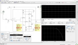
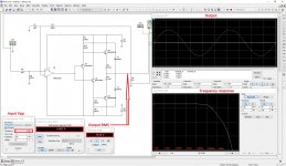
I was wondering if anyone could take a quick look at this circuit of mine. I want the op-amp to be able to supply the base current during the positive swing so allow for high output voltage so I placed a diode between the op-amp output and the base of Q3. This works fine, but it does lead to a little bit of crossover distortion as can be viewed in the image below. Is it possible to get rid of this distortion, or perhaps it's not really something to worry about? I thought of using a cap instead of a diode, but that led to some weird results (second image) including even worse crossover distortion that I can't really account for. Please pay no attention to the type of components used, they are only for simulation purposes, I'm asking from a pure topology standpoint.
LTspice simulation:
Title: * C:\Users\Torri\Desktop\Class AB amplifier.asc Date: Sun Feb 26 05:44:3 - Pastebin.com
An externally hosted image should be here but it was not working when we last tested it.
An externally hosted image should be here but it was not working when we last tested it.
LTspice simulation:
Title: * C:\Users\Torri\Desktop\Class AB amplifier.asc Date: Sun Feb 26 05:44:3 - Pastebin.com
Hi Plecto,
What kind of the op-amp are you trying to use?
I mean - if you use some power op-amp, like LM675, you don't need a buffer at the output - it drives 8 ohm load by itself with rather high quality.
If you use some low-power op-amp, you need a better design of the buffer. Why do designers use the drivers, or even [pre-drivers + drivers] combination in front of an output pair? Base currents, right? Having your buffer consisting of only a pair of the power devices, you have rather high base currents, resulting in the low input impedance of the buffer, strongly modulated in sync with the output signal.
Very difficult load for a low-power op-amp.
Cheers,
Valery
with just the cap you only have the 10k pullup for your upper Q average DC/cycle i_b
depending on requirements just use chip amps like LM3886, parallel if needed - likely heatsink area will be the biggest cost and it doesn't change with whatever PA chip or discrete Q if Class B
another composite op amp/discrete Q approach is using common emitter output Q driven by the op amp supply rail currents - but many Spice op amp models fail to give correct PS current, only a very few do the stability right for dynamic op amp PS Voltage
I want the amp to be stable at unity gain and I want to be able to manually adjust the bias current which is the reasons I have chosen this design.
Could you elaborate a little bit on that? What do you mean drive the transistors with the op-amp supply rail current? How is that different from the design I already have?
I could go with a low forward voltage schottky diode and lower the values of R5 and R6 as low as possible so that the crossover distortion only happens close to maximum current output, it probably won't be audible anyway I hope 🙂
another composite op amp/discrete Q approach is using common emitter output Q driven by the op amp supply rail currents - but many Spice op amp models fail to give correct PS current, only a very few do the stability right for dynamic op amp PS Voltage
Could you elaborate a little bit on that? What do you mean drive the transistors with the op-amp supply rail current? How is that different from the design I already have?
I could go with a low forward voltage schottky diode and lower the values of R5 and R6 as low as possible so that the crossover distortion only happens close to maximum current output, it probably won't be audible anyway I hope 🙂
Just skimming over the circuit...
Have you tried increasing the quiescent current in the output stage by lowering R2 ?
Keep the cap, ditch the diode, and you could experiment with a resistor from opamp output to speaker output. Something low, say 22 ohm as a guesstimate starting point.
No matter what opamp and all, you have to overcome the inherent dead zone of the output stage.
Compensating to operate at unity gain could be done by increasing the 'noise gain' of the chosen opamp if needed.
Just a quick skim through as I said 🙂
If you insist on OPA5551 with a buffer - this is something that will work, giving you up to some 12V RMS at the output.
If you need higher swing / lower distortion, you need a more sophisticated buffer.
Chips like LM675 or LM3886 will give you very good results with much less parts anyway 😉
If you need higher swing / lower distortion, you need a more sophisticated buffer.
Chips like LM675 or LM3886 will give you very good results with much less parts anyway 😉
Attachments

I want the amp to be stable at unity gain and I want to be able to manually adjust the bias current which is the reasons I have chosen this design.
you can do both with parallel chip amps
"noise gain compensation" allows unity gain - but seems pointless for audio amp driven from 2 Vrms consumer source
and parallel, R summed outputs can be biased push-pull by giving them a small DC offset, you could go all the way Class A, obviously a PA would used different Vos, smaller summing R

for the composite CE output, Walt's OP Amp Applications Handbook was handy http://www.analog.com/en/education/education-library/op-amp-applications-handbook.html
Attachments
Last edited:
I love that circuit of yours jcx 🙂 The bias current would then be 0.7/(R1+R2)? And the only thing limiting the output voltage swing would be the R1 and R2 drop pluss the limitations of the amp chips used? What is the purpose of C1 though? I'm also having a hard time understanding what "noise gain compensation" is though, would that be the C2 doing this compensation? Simply limiting the bandwidth? Is it impossible for an amplifier chip to start oscillation in the audio band in a configuration like this?
vzaichenko:
LTspice just flat out fails when trying to simulate that circuit 🙁 I don't quite understand the workings of it though, how is the bias current adjusted?
vzaichenko:
LTspice just flat out fails when trying to simulate that circuit 🙁 I don't quite understand the workings of it though, how is the bias current adjusted?
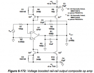
The circuit from jcx is really for high impedance loads but it is halfway toward something like the ancient Elektor current dumping amp.
This was designed to use Darlington outputs (I used discrete Darlingtons)
Clean up to clipping.
This was designed to use Darlington outputs (I used discrete Darlingtons)
Clean up to clipping.
Attachments

I love that circuit of yours jcx 🙂 The bias current would then be 0.7/(R1+R2)? And the only thing limiting the output voltage swing would be the R1 and R2 drop pluss the limitations of the amp chips used? What is the purpose of C1 though? I'm also having a hard time understanding what "noise gain compensation" is though, would that be the C2 doing this compensation? Simply limiting the bandwidth? Is it impossible for an amplifier chip to start oscillation in the audio band in a configuration like this?
vzaichenko:
LTspice just flat out fails when trying to simulate that circuit 🙁 I don't quite understand the workings of it though, how is the bias current adjusted?
That was a simplified version of double-bootstrapped diamond buffer, running at roughly 80mA idle current (all 4 transistors must be placed on the same heatsink).
Attached is a high-quality (low distortion) version of the buffer, running in one of my amplifiers - here you can adjust the bias. This one is designed for HexFET output devices, however it can be adapted to BJT ones.
Attachments
> 200mA drive capability so there are no limitations there
As said, the long-term feed to the upper device is 2.5mA, unless you SLEW the opamp 1.2V very violently.
What you want is a current source at 150mA and high compliance. (Not a 150 Ohms resistor). That is a heap of power.
When working from resistance-couple (what this is) into 8 Ohms, you usually want more current gain than single power devices have. Why not Darlingtons? Has worked for others.
I don't know why the fuss about unity-gain compensation. The OPA551 is unity gain stable. Throwing emitter followers in the loop rarely incites trouble.
The 50-cent fix for the crossover would be a capacitor. This will charge-down at FULL output, and maybe in a half-cycle of deep bass. But I think for speech/music it will be inoffensive. Certainly smoother than slewing a 15V/uS amp 1.2V on every cycle. R5 should probably be <1K, not 10K.
Attachments
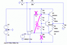
I think I got it 🙂 R5 and R6 has to be low enough to supply the average base current required, I think 1k should do it for this particular circuit. Even with 1k resistors and a capacitor instead of a diode, I still get crossover distortion when the voltage is decreasing. The blue graph shows the output of the op-amp. Knowing ohm's and kirchoff's law isn't enough to completely wrap my head around circuits like these, I often have a hard time understanding the values of every voltage drop and current 🙁
The talk about unity gain stability was for chip amps like the LM3886 by the way.
An externally hosted image should be here but it was not working when we last tested it.
The talk about unity gain stability was for chip amps like the LM3886 by the way.
Have you set an appropriate quiescent current in the output stage?
With 0 amplitude input signal, plot the current through R4 and R3. Adjust R1 and R2 until you get about 200mA current. I suggest starting with R2=1k and R1=1k and then adjust R2 until the quiescent current is correct.
I would also add bootstrapping capacitors to R5 and R6. Split R5 and R6 in two. Add a 470uF capacitor from the split to the output. As seen in figure 6a here: Elliott Sound Products - Audio Power Amplifier Design Guidelines
Hi Plecto,
For good performance you're looking for, you need:
- constant current sources instead of resistors at the buffer input;
- preferably symmetric drive circuit at the input.
My simple schematic in post #7 utilizes both of these things.
Simple CCSs are arranged with double bootstrap (capacitors, driven by the output.
The fact LTSpice crashes with this circuit, means most likely you're using some incorrect models.
You don't need to adjust the bias there, however, if you still like to - you can do it to some extent by adjusting the values of R7, R8, R10, R11 and to some extent - by adjusting the values of emitter resistors R2, R3. As is, it will run at around 70-80mA, demonstrating no visible crossover distortion.
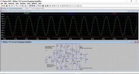
Attached are 2 screenshots from my Multisim simulation:
1) Static picture - note the idle currents;
2) Running a 1KHz sine wave through the circuit.
BTW, your output pair 2N3055/D45H11 is not as good for the purpose, especially at higher frequencies. They are not that complementary, higher base currents, higher capacitances, etc.
For good performance you're looking for, you need:
- constant current sources instead of resistors at the buffer input;
- preferably symmetric drive circuit at the input.
My simple schematic in post #7 utilizes both of these things.
Simple CCSs are arranged with double bootstrap (capacitors, driven by the output.
The fact LTSpice crashes with this circuit, means most likely you're using some incorrect models.
You don't need to adjust the bias there, however, if you still like to - you can do it to some extent by adjusting the values of R7, R8, R10, R11 and to some extent - by adjusting the values of emitter resistors R2, R3. As is, it will run at around 70-80mA, demonstrating no visible crossover distortion.
Attached are 2 screenshots from my Multisim simulation:
1) Static picture - note the idle currents;
2) Running a 1KHz sine wave through the circuit.
BTW, your output pair 2N3055/D45H11 is not as good for the purpose, especially at higher frequencies. They are not that complementary, higher base currents, higher capacitances, etc.
Attachments
Hi vzaichenko,
I agree on most of your points. However I am curious about your circuit, have you actually built it or have you just simulated it? Because I think it will be very hard for you to maintain a constant idle current over time and temperature with this circuit. And R7, R10 and so on will have to supply the entire base current of the output transistors making it quite inefficient.
I agree though that the amplifier of the thread starter will not be very useful without driver transistors. He should add a darlington EF or CFP as shown in figure 7 on Elliotts page.
Hi vzaichenko,
I agree on most of your points. However I am curious about your circuit, have you actually built it or have you just simulated it? Because I think it will be very hard for you to maintain a constant idle current over time and temperature with this circuit. And R7, R10 and so on will have to supply the entire base current of the output transistors making it quite inefficient.
I agree though that the amplifier of the thread starter will not be very useful without driver transistors. He should add a darlington EF or CFP as shown in figure 7 on Elliotts page.
Hi Ojg,
I have built a headphone buffer based on that kind of circuit long time ago. It's thermally stable - the drivers, being placed on the same heatsink with the output transistors, act as a bias servo.
A more sophisticated circuit, shown in post #11, is a part of one of our well-tested designs (VHex+ series, BiTurbo version):
http://www.diyaudio.com/forums/solid-state/294632-sons-vhex.html#post4782719
It can also work with no spreader within certain range of power levels, however, I have added the one for avoiding any possible temperature-related issues in case somebody decides to really abuse the amplifier 😉
Cheers,
Valery
It might produce some power without darlingtons or driver transistors, if the 2n3055 is a modern 20 gain part instead of a 1975 5 gain part. The DH45 might have some significant gain too. I've got some D44R2 from original 70's GE run and they are significant gain at 100 ma anyway.
I can't believe people are suggesting darlingtons after all the negative ink I've seen on here about them on the LM49810 thread. Isn't there supposed to be a big advantage of having 100 ohm base charge bleedoff resistors to rail with discrete drivers?
I'm a member of the "make something of what you have" club too: Instead of ordering some perfect transistor that is stocked only in Russia or from a counterfeit printer who will silk screen you any number you want on some ****y part. There has only been about 2 seconds of the last 100 record albums I've played where I can hear the difference between fast OEM driver transistors on one channel, and the 3 MHZ Ft TIP41/42C ($.38 each) I used on the other channel.
Last edited:
It's thermally stable - the drivers, being placed on the same heatsink with the output transistors, act as a bias servo.
Thank you, this is an important point!
if the 2n3055 is a modern 20 gain part instead of a 1975 5 gain part. The DH45 might have some significant gain too. I've got some D44R2 from original 70's GE run and they are significant gain at 100 ma anyway.
OK, sure.
However - 2N3055/MJ2955 is a complementary pair of one kind (higher power, lower beta, low fT), D44H11/D45H11 is a complementary pair of the other kind (lower power TO-220 package, higher beta, 10 times higher fT).
Each pair is possible to use with decent results, but using a pair like 2N3055/D45H11 is really suboptimal as those are way too different 😉
Links to the datasheets as a reference (both are OnSemi):
http://www.onsemi.com/pub/Collateral/2N3055-D.PDF
http://www.onsemi.ru.com/pub/Collateral/D44H-D.PDF
- Status
- Not open for further replies.
- Home
- Amplifiers
- Solid State
- Having a slight issue with my class AB output stage