If you wanted to build an amp without using a pcb design, could you use the general layout of the amp's schematic and hard wire it that way assuming that you reduce the distance between components to the very minimum possible?
If this is possible what are the pitfalls and what should one avoid and what should one look for. Or is it really not a good idea. I am thinking of simple amps like the JLH, Hiraga et al.
Did I see somewhere an amp that was hard wired on one side of a single sided pcb that used the copper side for the ground plane?
Any thoughts on this? I tried a search but did not find anything.
🙂
To answer your question, yes, it's very workable.
Downsides and pitfalls. OK you did ask 🙂
It will look a mess.
You would have to support various components to prevent stress and fractures on wires.
You still have to get the grounding etc correct... wires to the correct places... and in fact point to point wiring could make that aspect easier.
There are advantages too, such as less stray inductance and capacitance between adjacent PCB print etc. It might run cooler... parts in free space.
Would I do it,
Nooooooo 😉
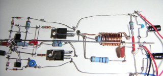
An alternative approach which works reasonably well is to use a plain "PCB" with point-to-point wiring below. See my chipamp construction in http://www.diyaudio.com/forums/chip-amps/79303-chip-amp-photo-gallery-67.html#post1545017
This has the advantage of maintaining some rigidity but without the need for a PCB design. When viewed from the component side, there is no suggestion that the board isn't etched. Insulated wire jumpers can also be concealed in this way.
Regards,
Steve
This has the advantage of maintaining some rigidity but without the need for a PCB design. When viewed from the component side, there is no suggestion that the board isn't etched. Insulated wire jumpers can also be concealed in this way.
Regards,
Steve
Hi Mooly,
why would you not try it; any particular reason? It would not be a mess if you took some time keeping all wires and components straight and aligned accurately with each other.
Hi stormsonic,
yes that is what I am talking about. What is the amp pictured? Did it work to your satisfaction? Does the layout follow the schematic?
Hi currentflow,
very nice build of your amp; like it.
What about the idea of using a single sided pcb and then hard wiring the components on one side and using the copper side for the ground plane. I have seen this on a photo on this site somewhere.
everything used to be made point to point with a few terminal strips thrown in, including colour tv's. Circuit boards are labour saving devices and increase reliability, and repeatability of performance. Buy a piece of vero board, a circuit board with tons of holes and little if no copper, and go for it. I used to make tons of little "air suspension" as my friends and I called it, circuits.
i would like to p2p a dx blameless es amp by carlos, the schematic although is readable you can get quite confused. I was looking for a program that you can upload a pcb diagram and then proccess it to layout your circuit as p2p then you can just copy it. Unfortuntely i dont know if this program exists tried searching for it but unsuccessful.
Hi jerryo,
Thank you for your kind comment. It's debatable as to whether having a ground plane is particularly beneficial at audio frequencies. Perhaps more important is the use of correct earthing / star grounding techniques and low-impedance interconnects for high-current carrying paths. A good layout will also assist circuit stability.
Plain perforated board would perform identically (electrically) to my P2P technique although it's somewhat less aesthetically pleasing.
Regards,
Steve
schematics are drawn for human readability - not to optimize electronic circuit performance - circuit implementation in pcb layout or prototype is a critical part of the circuit's performance
power is usually shown top and bottom of the page for +,- most of the time they should be distributed in closely spaced traces to reduce the loop area that radiates magnetic feild
gnd also needs attention with ground plane being the simplest but star gnd principles are better for power circuits
power and gnd sould be planned with an eye to where the current flows and what it does in the "non schematic" parasitic RLC of real wires and how they couple to the circuit
sensitive feedabck or high impedance nodes don't have to be short on paper - in the real world you want to know which nodes are sensitve and how they drive parts placement for the best results
there are several prototyping techniques for building without a pcb layout
perf boad gives rigid mounting, can be had with clearance hole gnd plane for lower noise in low level circuits
"dead bug" on gnd plane is used for some high speed analog circuits
some pretty point-to-point air wiring can be better than a 2-d pcb for some parts of a circuit - but you won't likely get there by letting the schematic drawing be your physical layout guide
a possible aid to perfboard or ~ 2-d layouts could be to use a pcb layout package with "rats nest rubber-banding" mode - the part outline pads are shown with straight wire that moves with the part's releative position for all schematic connections, by moving, grouping and rotating parts you can minimize sensitive node length before you start routing
the free CadSoft Eagle demo package may be good enough for this use
Last edited:
Hi Mooly,
why would you not try it; any particular reason? It would not be a mess if you took some time keeping all wires and components straight and aligned accurately with each other.
I just wouldn't.
Again you have asked the question 🙂 and the answer is that to me it would always look a mess. I work to far higher standards than that.
But as I say it is workable, and done correctly should not give problems... and as long as you are happy with it, then that is all that matters.
It's so easy to design and make your own PCB's these days.
Have a look at posts # 22, 23 and 31.
http://www.diyaudio.com/forums/headphones/160646-germanium-single-ended-class-headphone-amp.html
Don't let that put you off... build it, enjoy, learn... and always strive for better.
🙂
The mpp thread by Joachim Gerhard has many pictures of his deadbug amplifiers. Joachim builds most/all of his preamp designs that way. Take a look, there are many examples. This is just one:
http://www.diyaudio.com/forums/analogue-source/154210-mpp-59.html#post2140489
http://www.diyaudio.com/forums/analogue-source/154210-mpp-59.html#post2140489
Why not buy some stripboard ?
That has copper tracks in parallel with each other and holes every 1/10 inch.
I have used it successfully for numerous designs to test them out before going to pcb.
That has copper tracks in parallel with each other and holes every 1/10 inch.
I have used it successfully for numerous designs to test them out before going to pcb.
mooly
Is that the only reason? I would think it would be easier to do point to point wiring for a one off design than PCB, not to mention: a lot easier changing things after the fact, being able to do complicated (needing multiple layers on a pcb), being able to use higher gauge wire, lower inter trace capacitances, probably missed something.
and the answer is that to me it would always look a mess
Is that the only reason? I would think it would be easier to do point to point wiring for a one off design than PCB, not to mention: a lot easier changing things after the fact, being able to do complicated (needing multiple layers on a pcb), being able to use higher gauge wire, lower inter trace capacitances, probably missed something.
mooly
Is that the only reason? I would think it would be easier to do point to point wiring for a one off design than PCB, not to mention: a lot easier changing things after the fact, being able to do complicated (needing multiple layers on a pcb), being able to use higher gauge wire, lower inter trace capacitances, probably missed something.
You keep pushing me on this one 🙂
It's amateurish... part of the satisfaction of building a piece of kit is (to me) turning out a decent PCB. Whatever I build I want to look as professional as possible... and it's through being a member of DIY and looking at what some folk turn out that has encouraged me to "up my game"... second best is never good enough.
I realise many won't take things that seriously or are just happy to fiddle around with a design and get some satisfaction from getting it to work... that's fine 🙂 but it's not me.
I did this PCB just to "evaluate" a particular design... there's no other way.
http://www.diyaudio.com/forums/soli...-built-listened-d-selfs-precision-preamp.html
As to making it easy to change things... if that's the case and is something you need to keep doing then the "design" wasn't "right" in the first place.
Hey Mooly ,I did build that preamplifier ! I made the PCBs ,one for the circuit and one for the pots , and flat multi-wire to connect them. It worked together with a mosfet amp for some months ...The parametric equalizer didn't make dramatic changes when shifting frequencies ,then when the treble controls ceased to function , I dismantled everything ...😛
then when the treble controls ceased to function , I dismantled everything ...😛
🙂 There's just no answer to that one is there 😉
It's amateurish... part of the satisfaction of building a piece of kit is (to me) turning out a decent PCB. Whatever I build I want to look as professional as possible... and it's through being a member of DIY and looking at what some folk turn out that has encouraged me to "up my game"... second best is never good enough.
I'm with you there Mooly. To me, if it doesn't look professionally made, it's not good enough. Here my latest PCB:
Attachments
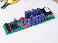
I'm with you there Mooly. To me, if it doesn't look professionally made, it's not good enough. Here my latest PCB:
That looks really good 🙂
Hi amc184 and Mooly,
I understand exactly where you are coming from. I am a perfectionist is some aspects of my life and therefore continuously strive to increase the quality of what I do. I admire your approach.
But, I simply do not have the time or in fact the skill to design and manufacture pcb's; I can however use a soldering iron effectively. I have very little patience with computers. I will make my own pcb's one day but they will be from established designs and not my own.
Cheers
- Status
- Not open for further replies.
- Home
- Amplifiers
- Solid State
- Hard wire as per schematic!