Hi can anyone please clear up a question about the ground symbols on this schematic. I have highlighted the offending symbols in yellow and put my guess next to them. Also you will notice two back to back electrolytics on the input. would there be any benefit in sound quality if i replace these two capacitors with one polypropolene LCR 8mf audio grade cap.
regards Ian
regards Ian
Attachments
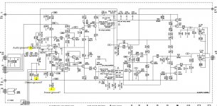
The two caps is series whould result in 5 ufd with the idea that the combination would be non polarized (that is why the polarity is back to back). A replacement could be 5 ufd non polorized in you favorite type. The ground symbols are confusing, there shoud be some indication on the drawing. Look for some note.
Thanks Fire chief.
I have had a look at the psu schematic and have found the symbol i have marked as power ground is the 0 volt junction between the two large res caps in the psu. so i guess power ground. as for the input caps i mentioned i did understand why the caps are back to back and that the sum of both equals 5uf. to replace the two 10uf input caps will mean i have to remove them and replace with links as there is no room to fit the larger film caps in that location .i was planning on locating them near to the input connectors.
After the input caps there is a 1k resistor that conects to the inverting input of the opamp wich i understand from my extensive reading i have done on this forum to be virtual ground. Now the two caps and the resistor to ground create a high pass filter with a corner frequency of 31.83Hz. the spec sheet of this amplifier says it has a frequency response starting at 7 Hz. The confusion grows
Your guesses for the different grounds seems correct to me, just from looking at the schematic. But I think it is R102 not R101 that's used for the fc formula, with R101 being a small enough value that it can be ignored.
Your guesses for the different grounds seems correct to me, just from looking at the schematic. But I think it is R102 not R101 that's used for the fc formula, with R101 being a small enough value that it can be ignored.
Thankyou Sofaspud.
I recalculated the cut off frequency using the value of R102 47k5 and 5uf cap and i get the cut off frequency of 0.67 Hz and a time constant of 0.2375 second.
If i calculate with 8uf (as these are what i have) I get cut off frequency at 0.42 Hz and a time constant at 0.38 second. Do you think it would be ok to use the 8 uf film cap instead of the two back to back electrolytics.
After reading many posts on this forum i am led to belive that so called audio grade polyprop caps are better in this position. Size and cost left out of the equation.?
and finallly just to clear things up a little is the inverting input of the opamp not seen as virtual ground as it is in the lm3886.?
Best Regards Ian
Electrolytics are best left out of the signal path - that's pretty much universally agreed upon (See? It does happen!🙂). Larger value film caps are more of a premium item and nowhere near as common as electrolytics. The 8uF film would be the caps to use.
I don't really have an answer for your op amp question. It depends on how it is connected. In the circuit above, the inverting input is connected to DC ground thru R102; the noninverting input is connected to AC ground thru C101. At least I think that's correct.
I had thought an op amp amplifies the difference on its inputs, then I find a circuit with the inputs tied together. What's going on? Is that a unity gain configuration? Oooo my head hurts🙂
I had thought an op amp amplifies the difference on its inputs, then I find a circuit with the inputs tied together. What's going on? Is that a unity gain configuration? Oooo my head hurts🙂
An opamp with inverting and noninverting input tied together obviously isn't going to be useful. A differential voltage of 0 amplified by any gain will have 0 as result.
Did you mean output tied to inverting input? If so, that's a voltage follower and that has a gain of 1.
An opamp with inverting and noninverting input tied together obviously isn't going to be useful. A differential voltage of 0 amplified by any gain will have 0 as result.
Did you mean output tied to inverting input? If so, that's a voltage follower and that has a gain of 1.
To be pedantic that is not quite true 😉
Tying the inputs together means that the input Vos (offset error), almost no matter how small, will get amplified by the open-loop gain causing the ouput to whack against one of the power rails.
Cliff (pedant)
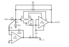
If You look at the schematic i posted . the the inv and non inv inputs are not tied together. I have another question to ask about the schematic i posted . is it using what is known as nested feedback? to me it looks simler to the myref chipamps that can be found on this forum.
Regards ian
Regards ian
madtecchy, I don't think yours is a nested op amp circuit. "Nested" is, I believe, another term for having 2 op amps with one inside the feedback loop of the other (as seen in this composite amplifiers thread). Your circuit reminds me more of the headphone amp circuits that include a discrete output buffer. I haven't checked out the MyRef circuits yet, but it did come up in the aforementioned composite amp thread.
(see Linear Technology AN-21 Composite Amplifiers by Jim Williams, Figure 2, for the OT stuff)
(see Linear Technology AN-21 Composite Amplifiers by Jim Williams, Figure 2, for the OT stuff)
Last edited:
To be pedantic that is not quite true 😉
Tying the inputs together means that the input Vos (offset error), almost no matter how small, will get amplified by the open-loop gain causing the ouput to whack against one of the power rails.
Cliff (pedant)
Yep, in the real world it will. I was talking about the ideal opamp.
Last edited:
C111 should connect to C112 and this junction connected to Zero Volts at the Main Audio Ground (MAG)
Similarly c119, 120, 121,122, 123, 124.
C113 would also connect to the on board Zero Volts.
All these nF capacitors should connect using the very shortest traces/wires you can design into the PCB.
I would class all these Decoupling and Zobel Grounds as Power = dirty Grounds.
The intermediate groundings around the pre-drivers and such carry much lower currents and these currents tend to follow the "slow" audio signals. I would group these together as Clean Ground.
At the input, some of the connections go off PCB via the J104, 107 & 108.
Try to identify which of these Grounds are really Signal Grounds. Group them together and use a separate wire to connect this Signal Ground Star to the MAG. Connect both R102 & C101 to Signal Ground.
Finally, the opamp is shown in inverting mode. The opamp is inside a composite topology and note the the NFB goes to the +IN pin and then via the DC blocking caps to Signal Ground. This tells us that the composite amp behaves as a non-inverting amplifier.
PIN2, labeled as -IN is actually the +IN pin of the composite amplifier. As such, R102 acts as Rin and is not a "load" on the inverting input pin.
Can you identify if C107 & R104 are connected to the chassis at the input socket?
Last edited:
Hi Andrew
Thankyou for taking time to descibe the input part of this circuit.
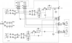
It is a comercial amplifier made by ECLER. so all conections are already made. And as such has no hum or buz problems. Could you please tell me the inputimpedance of this circuit or at very least how to calculate it . Once again thankyou for the very informative reply.this amplifier also has a seprate pcb with a ballanced line input and this gives the amplifier its published input impedance of 10Kohm
Thankyou for taking time to descibe the input part of this circuit.
It is a comercial amplifier made by ECLER. so all conections are already made. And as such has no hum or buz problems. Could you please tell me the inputimpedance of this circuit or at very least how to calculate it . Once again thankyou for the very informative reply.this amplifier also has a seprate pcb with a ballanced line input and this gives the amplifier its published input impedance of 10Kohm
Hi Jitter thanks for the very good usless imformation. This is the real world not the ideal one
And that brings us back to my original point: in the real world you won't see opamps with both inputs tied together, as that's ... ehm... well... useless...
I'm really curious where sofaspud saw that...
Last edited:
If you would like to take it up with sofaspud that is your perogative. I suggest you use private msg to ask him about it . You could even start a new thread.
Rather than remove the balanced input, I'd suggest you simply bypass it.
The input to the Amplifier is at the two back to back electrolytics (C103) or pin3 of j107.
Open the existing connection and connect your unbalanced feed here instead.
I would also suggest you remove the electrolytics and substitute a metalised film cap. A cheap one of the correct value will be better than any pair of electros. Later you can experiment with polypropylene and/or teflon in film+foil or metalised film.
R102 sets the input resistance. I can't read the value.
R101 is in series before it so for arithmetic accuracy that 1k0 should be added. Then you can also add in the actual input stage impedance in parallel to R102.
For simplicity ignore these corrections.
4u7F and 22k for Rin would give ~103ms RC time constant. You can choose to vary this from 20ms to 200ms to suit your taste.
But, you must change the NFB capacitor to match. The RC for NFB >=sqrt(2) * Input RC
That is equivalent to: "change C101"
Last edited:
Thankyou Andrew.
I will get on with that. I have a couple of LCR audio grade polyprops I can use.I just need to find somwhere to fit them. there is a space that they might fit into near the input sockets and well away from any large current sources. I will report back to let you know when i have done the mod.
Regards Ian
- Status
- Not open for further replies.
- Home
- Amplifiers
- Solid State
- ground symbol confusion