Hello,
I have a PCM1704K based dac and the PCB was whatever I found at the time. It has many ground plane areas on the 2 layers, some floating (not connected) some grounded.
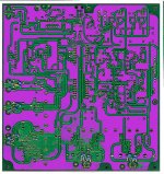
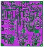
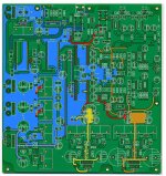
Images attached, purple shows the ground planes and highlights show the area where they are connected.
I have read numerous articles on grounding and I'm leaning towards a single ground plane. Article
However I'm wondering wheter to leave the planes as is or to cut some traces and connect them differently. The two options are star-ground or jumpers to simulate one single ground plane.
If i go for jumpers - then obvioussly they would be at the edges of the current areas. If i go for star shoud I connect to the center of the areas instead ?
What should I do for the smaller areas that are 'floating' ie: not connected?
Thanks.
I have a PCM1704K based dac and the PCB was whatever I found at the time. It has many ground plane areas on the 2 layers, some floating (not connected) some grounded.
Images attached, purple shows the ground planes and highlights show the area where they are connected.
I have read numerous articles on grounding and I'm leaning towards a single ground plane. Article
However I'm wondering wheter to leave the planes as is or to cut some traces and connect them differently. The two options are star-ground or jumpers to simulate one single ground plane.
If i go for jumpers - then obvioussly they would be at the edges of the current areas. If i go for star shoud I connect to the center of the areas instead ?
What should I do for the smaller areas that are 'floating' ie: not connected?
Thanks.
Attachments
Star grounds are no good for digital.
I would cut down on the width of your signal tracks firstly, they do not need to be that wide, that will allow for better copper pour of the ground.
Secondly stich the top and bottom grounds together using numerous stiching vias to create as near as possible a contigous plane.
Unconnected area of copper is a no no.
Dont realy require curved tracks, benefits will be minimal at these frequencies if any.
Design would benefit from moving the components much nrearer together.
Why so many largish electroylitics?
Thanks,
I'll get to it asap.
The reason for the electrolytics near the edges is that those a power regulators. There are 6 separate rectifiers+regulators.
Just to be clear you mean I SHOULD connect the floating areas to ground, right? Except maybe when too small.
Agree the design is too far appart but not much I can do about that...on this project.
Yes, any unconnected copper is bad practice, tie the ground areas together with as many vias as possible without going crazy. If you cant connect small areas try and delete them.
Yes, any unconnected copper is bad practice, tie the ground areas together with as many vias as possible without going crazy. If you cant connect small areas try and delete them.
+1 Remember that at RF frequencies EVERTHING is an antenna/waveguide/resonator, all due to simple physical geometry and its relationships with the wavelengths involved.
better to have areas of ground tied together with multiple vais, better for signal integrity, provides lower impedance return and allows return current to follow more closely the path of least inductance, which will be the path under the trace. Also having multiple vias will reduce the area or size of a feature electronicly in relation to wavelength, increasing the frequencies that may cause you problems, for this reason use at least two vias per area at opposite ends to avoid creating a diplole structure.
If you PCB manufacturer can handle it some 0.3mm vias would be nice, but for costs you may have to use 0.5mm finished hole vias.
If you PCB manufacturer can handle it some 0.3mm vias would be nice, but for costs you may have to use 0.5mm finished hole vias.
I have separate power supplies (6 or so) and associated regulator circuites on the same board.
Should I have 6 ground planes, one for each 'area' supplied or one unified ground plane? (Nevermind digital/analog).
Thanks.
Should I have 6 ground planes, one for each 'area' supplied or one unified ground plane? (Nevermind digital/analog).
Thanks.
Chisel PCB Traces
Any good ideas on how to chisel out PCB traces - planes ?
I was thinking some sort of hobby chisel.
Not sure worth it. Top is already populated, might be worth just connecting all the ground planes.
Bottom - I'd rather remove all the 'floating' ground planes since they are useless. The IC's (PCM1704 and DF1704) are on daughter boards, not great practice, so no point to have a ground plane 5mm below.
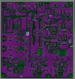
Attached, PCB TOP and Bottom (post below) - green areas are floating, except on the right side (Analog I/V) where I did not bother to go in details). Blues and Yellows are Grounds, red are +V and Greys are -V.
There is a huge amount of floating areas.
In principle this PCB is crap, but sounds good, so it's a salvage operation.
Thanks
Any good ideas on how to chisel out PCB traces - planes ?
I was thinking some sort of hobby chisel.
Not sure worth it. Top is already populated, might be worth just connecting all the ground planes.
Bottom - I'd rather remove all the 'floating' ground planes since they are useless. The IC's (PCM1704 and DF1704) are on daughter boards, not great practice, so no point to have a ground plane 5mm below.
Attached, PCB TOP and Bottom (post below) - green areas are floating, except on the right side (Analog I/V) where I did not bother to go in details). Blues and Yellows are Grounds, red are +V and Greys are -V.
There is a huge amount of floating areas.
In principle this PCB is crap, but sounds good, so it's a salvage operation.
Thanks
Attachments
Last edited:
- Status
- Not open for further replies.
- Home
- Source & Line
- Digital Source
- Ground plane - Upgrade