Hello.
I've been thinking of how to make it easy to prototype a ground plane circuit. One obvious option is dead-bug style. However the ground plane is easy to short to, so the leads can't be too close. This seems to me to defeat the purpose of a ground plane at times.
I thought a good idea was to cover a board with a fiber/paper-based tape. Since it's not plastic it would not melt, but maybe smoke a little while soldering, and wouldn't mess up the iron if touched. When a ground connection needed to be made, some of the tape could be cut off by an exacto knife or screwdriver. This way the components could be right up next to the ground plane, and you could use their own leads as PCB traces.
BTW, would it be a problem to use this method on a double-sided PCB? IE, the third copper plane would act like a shorted turn in a transformer, and ruin the ground plane effect where the current follows the "path of least inductance".
What do you think? What kind of tape should I use and where to get it?
Thanks,
- keantoken
PS: I graduate on the 4th, and no, I haven't forgotten about the Goldmund project!
That website is a zombie.
I thought fiber/paper tape could be useful since it's easy to glue components to...?
Thanks,
- keantoken
I thought fiber/paper tape could be useful since it's easy to glue components to...?
Thanks,
- keantoken
I do exactly the same as Elvee. Self adhesive copper tape (it's not cheap!), which can be overlapped to cover large areas - put a dab of solder or two on the 'seam' so as to ensure good DC continuity. Make small square holes with a scalpel to pass the legs of the components through. Sounds like hard work, but a great advantage is that you have a ground to solder to wherever you want it which I think offsets the effort in making the holes. And all the while you know that your prototype is going to work practically as well as one built on a PCB.
In fact, I almost never use sticky copper: I start with a blank single-sided PCB I use upside down.
Sorry Elvee, got the wrong end of the stick. I was referring to a way of working with Veroboard and placing a groundplane on the component side.
Thanks for the advice.
What I want seems to be a convenient form of point-point wiring that is more controllable concerning parasitics. Pushing pins into holes seems tedious to me and would seem to make for longer lead lengths when an alternative is to simply solder the leads straight from point A to point B.
Am I too picky?
- keantoken
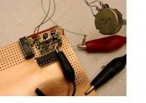
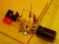
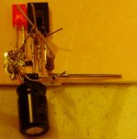
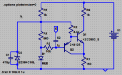
The idea seems to be a success, coupled with my recent discovery of SMD resistors. Here is a schematic and pics of the construction. This is the Baxandall Super Pair. I want to see if it oscillates, and if so, what it takes to stabilize it.
In the pictures I used masking tape. I also discovered that you can trace lines of solder along the tape, much like drawing your own circuit... VERY useful I think. However it may be difficult to remove the solder once it's on the tape.
My only problem is that my 25W iron has troubles soldering to the ground plane, which acts as a heatsink.
I still think this is a good question:
- keantoken
In the pictures I used masking tape. I also discovered that you can trace lines of solder along the tape, much like drawing your own circuit... VERY useful I think. However it may be difficult to remove the solder once it's on the tape.
My only problem is that my 25W iron has troubles soldering to the ground plane, which acts as a heatsink.
I still think this is a good question:
keantoken said:BTW, would it be a problem to use this method on a double-sided PCB? IE, the third copper plane would act like a shorted turn in a transformer, and ruin the ground plane effect where the current follows the "path of least inductance".
- keantoken
Attachments
Well, it doesn't oscillate. At least not below 20MHz. Oscillation at a higher frequency is definitely an option. It is also possible that the circuit won't oscillate but will exhibit dangerous resonance and phase behavior at HF that will throw off an amp. I could test this up to say 10MHz if I had my signal generator working but it is in need of a recap.
- keantoken
- keantoken
- Status
- Not open for further replies.
- Home
- Amplifiers
- Solid State
- Ground Plane Prototyping