Hi
What do I have to watch when making good pcb for ClassD amp?
Loops, ground and where to put (under chips)... that kind of things.
What do I have to watch when making good pcb for ClassD amp?
Loops, ground and where to put (under chips)... that kind of things.
As with any pcb design, you must be very aware of where currents will be flowing. In the case of a class d amp, the most critical areas are the output stages where there are high voltages and large currents with fast rise and fall times. Grounding, decoupling, keeping loop areas small, keeping sensitive circuitry/traces isolated from potential sources of noise/coupling, etc. all need to be taken into consideration.
Start with a general idea of what board shape/size you want, but do not constrain yourself to set dimensions unless you have to.
Surface mount parts are your friend (and really aren't any harder to solder than through hole parts!).
One layer boards are more difficult to design than two layer boards.
Route the power stage traces first and work backwards (output to input). Power stage traces include VDD, VSS, AND the ground returns!!!
Always be conscious of where ground currents will be flowing if a ground plane is used. Keep low current signal ground currents and ground sense points away from high currents flowing through ground planes.
Don't forget to take part placement into account for proper cooling. For example, TO220 devices will probably need to be attached to a heat sink and are usually positioned at the edge of the board.
There's much more, but that's a start. As has been said many times, pcb design is an exercise in compromise!
Hi
Ok I will keep all of this in my mind.
How about placing clock/sawtooth generator under the the comparator that makes PWM? Or should I just put everything on one layer and use other layer ground plane?
Another thing is how/where to connect together power and signal ground and how much apart should they be?
Now I have power coming to amp on each side of the board running almost from start of the board along whole board strait to fets on other side, having logic between them. Is that Ok?
Are only high current with high di/dt problem?
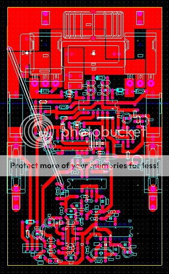
This is how board looks now

Ok I will keep all of this in my mind.
How about placing clock/sawtooth generator under the the comparator that makes PWM? Or should I just put everything on one layer and use other layer ground plane?
Another thing is how/where to connect together power and signal ground and how much apart should they be?
Now I have power coming to amp on each side of the board running almost from start of the board along whole board strait to fets on other side, having logic between them. Is that Ok?
Are only high current with high di/dt problem?
This is how board looks now
Hi
And what size of resistors to use. I have experience with SMD's but haven't done any board for myself. Also what else to put in smd, I was thinking of leaving power zener(for +/- voltages for chips) as they are.
And what size of resistors to use. I have experience with SMD's but haven't done any board for myself. Also what else to put in smd, I was thinking of leaving power zener(for +/- voltages for chips) as they are.
Hi luka. Many questions related to layout depend on other aspects of the design/layout but here are some general answers.
Also, can you post a schematic of your design?
The quality of the triangle/sawtooth waveform is directly proportional to the quality of the sound. Since this signal is compared to the audio signal you do want it close to the comparator, but you do not want the operation of one component to interfere with the other. For example, do not run the output of the comparator directly next to the input trace carrying the sawtooth waveform or other traces used to generate the sawtooth waveform.How about placing clock/sawtooth generator under the the comparator that makes PWM?
You are curently working on a 1 layer design so it may be easier to place all components on one layer and use the other layer as a ground plane. Others have done this with good success. classdfromru has some nice photos of his home etched boards and hand built circuits on his website. If you decide to use one layer as a ground plane remember to think about where ground currents will flow. You don't want a high output current pulse flowing through the same area as a ground sense point.Or should I just put everything on one layer and use other layer ground plane?
Ideally you want power ground and signal ground connected at one point. A good place to do this is near the speaker ground for a single ended design such as yours.Another thing is how/where to connect together power and signal ground and how much apart should they be?
This should be ok. Another good rule to follow is to have power and return traces running side by side, like the two conductors in a speaker cable. And if you must cross power traces with signal traces, cross at 90 degree angles to minimize coupling.Now I have power coming to amp on each side of the board running almost from start of the board along whole board strait to fets on other side, having logic between them. Is that Ok?
High di/dt and high dV/dt. They often go hand in hand though.Are only high current with high di/dt problem?
Resistor size depends on how much power they will have to dissipate. As far as SMD resistors go, you will generally find that 0603 size resistors will be rated to handle 1/10W, 0805 will be 1/8W, 1206 will be 1/4W, 2010 will be 1/2W, and 2512 will be 1W.And what size of resistors to use.
Almost everything is offered in a surface mount package these days. Whether or not you want to use the surface mount version depends on many things: available board space, cooling requirements, cost, rework capabilities, etc.Also what else to put in smd, I was thinking of leaving power zener(for +/- voltages for chips) as they are.
Also, can you post a schematic of your design?
Hi luka. Does the board you have shown in your picture work? If not, what doesn't work?
Also, what is the feedback node connected to? There is only one "FB" label on the schematic.
Also, what is the feedback node connected to? There is only one "FB" label on the schematic.
Hi
Sorry my mistake. This FB connects to out, this is post filter feedback. Yes amp works up to around +/-35v signal on output, then is goes crazy and puts +Vcc on output. I asked what could be wrong, and the answer was that it could be bad ground, so pcb badly done. I have +/-0.5v, 250kHz squerewave on supply node of 4060 if I look with scope only for AC signals. This is with no input signal. With input signal, spikes on this node became about +/-4v on top on those 15v even though I have I tantal cap.
Sorry my mistake. This FB connects to out, this is post filter feedback. Yes amp works up to around +/-35v signal on output, then is goes crazy and puts +Vcc on output. I asked what could be wrong, and the answer was that it could be bad ground, so pcb badly done. I have +/-0.5v, 250kHz squerewave on supply node of 4060 if I look with scope only for AC signals. This is with no input signal. With input signal, spikes on this node became about +/-4v on top on those 15v even though I have I tantal cap.
I figured you had used post filter feedback but just wanted to make sure.
That is some really bad ripple on the 15V supply line! Do you see similar ripple on the 10V and 12V supply rails? On the schematic the anodes of the positive regulator zeners and the cathode of the negative reglulator zener are not connected to ground. Are they connected to ground on the board?
The schematic doesn't show it but you should use a larger value electrolytic capacitor on each supply rail near the FETs. It doesn't appear that you are from the pictures. Try using at least 100uF (220uF to 470uF would be better) across each 47V rail close to the output FETs.
Hi
Never do things in hury, you will make them wrong. Positive regulator zeners and the cathode of the negative reglulator zener are connected to gnd.
Never do things in hury, you will make them wrong. Positive regulator zeners and the cathode of the negative reglulator zener are connected to gnd.
You see right. I had no where to put them, so there aren't any. I will put them just to see what will happen to that ripple. Ripple is present on every line, since all of them are elevated xxV from ground. Ground on my board is only about 2cm^2 big, just to have two fastons for supply and speakeruse a larger value electrolytic capacitor on each supply rail near the FETs
BWRX said:
Don't forget to take part placement into account for proper cooling. For example, TO220 devices will probably need to be attached to a heat sink and are usually positioned at the edge of the board.
Disputable point, for instance, i like to place to-220 (face down) at the bottom layer, and press PCB to the heatsink. On the UcD board, mosfets placed in the center also.
Hi
I plan to do that too. I will just place whole amp over 2-3mm Al plate the same size as board, unless I will go for 1HE hight
I plan to do that too. I will just place whole amp over 2-3mm Al plate the same size as board, unless I will go for 1HE hight
You might want to consider using several different power and ground wires, between the power supply and this board.
I would run separate power and ground wires to the board for each section that has relatively-large di/dt or dv/dt, and a separate set of power & ground wires for the low-level sections and the sensitive sections.
For the really noisy ones, you could consider using shielded multi-conductor cable, with the shield's drain-wire connected only on the power supply end, to ground.
And you can add EXTRA separate ground wires from PSU to board, for any "very sensitive" grounds, if needed.
Note that "ideally", every board ground and power point would have a separate wire, back to the PSU. That is not usually necessary, or practical, but should still be kept in mind as "the ideal". (But, of course, that wouldn't be true if ground return currents need to flow between two devices on the board, for example, in which case you probably wouldn't want them to have to go all the way to the PSU and back again.)
Obviously, then, too, the ground and power traces ON the board (and in your PSU, too) should be "shared" as LITTLE as possible, by currents from different circuits and devices. Every trace and wire has some distributed resistance and inductance. So, currents flowing through them always induce a voltage between any two points on the trace or wire, which increases with the length of the trace or wire. So, for example, a return current, in a ground trace or wire, that has large dI/dt, will induce a voltage with some corresponding dV/dt, between the ends of the trace or wire. So, if ALL of your return currents share the same ground wire back to the PSU, then, if there is a current with a large dI/dt, your board's GND will be a "bouncing" voltage. instead of a steady 0v, and the sensitive circuits that need a stable ground voltage might be badly affected. And the same type of thing is true for your power rails.
Maybe you can test it: On your board, try using your oscilloscope to look at the ground voltages, placing the probe tip on a board ground point and the probe's ground clip at the PSU's main ground return point, where the board's ground eventually connects to it (probably one side of a main filter cap). (Actually, it might be better to try to use two probes, and differential mode on the scope.) See if the board ground points for any relatively-sensitive parts of your circuit are stable. If they are not, but you think they need to be, then run a separate wire from the PSU ground point to that board ground point, OR, give the high di/dt ground returns, which are probably causing most of the problem, their own separate ground (and probably also power) wiring back to the PSU.
If you have a Spice simulation of your circuit, you can find out which points need separate wiring back to the power supply, by inserting a series R and L in each wire (e.g. using values from web-based calculators for wire and trace inductance and resistance). Then run your simulation and note the voltage variations at various ground and power rail points in your circuit. THEN try using a separate set of ground and power wires for your highest dI/dt devices, and check the other devices' ground and power voltages. You might be amazed. You could try it for "all combinations". But usually just separating the "worst offenders", and also the very sensitive ones, helps enough.
One other thing:
For your ripple problem, it might be a very big help if you put an inductor in series with each of the power rails, very near where they go to your high dI/dt or dV/dt devices, while the other parts of the circuit do not take their supplies through those inductors.
The inductors' value will depend on the frequencies involved. And you'll have to make sure they can handle the RMS current levels. But they can almost work miracles, sometimes, especially where a small frequency range is a problem.
If you have a spice simulation, especially one with the wiring and trace parasitic R's and L's as mentioned above, it might be easiest to find the best inductance values by trial and error, with simulations. But it will probably be somewhere between 10uH and 470 uH.
There are small chokes available, often no larger than a 1/2W or maybe 1W resistor, that might work well for your application, depending on the RMS currents involved. If you simulate them, make sure you include the DC Resistance for the inductors. You might also want to see what happens if you add a small resistor in parallel with each of the inductors.
Good luck!
- Tom Gootee
http://www.fullnet.com/~tomg/index.html
-
Hi
So what you are saying I should use 3 wires that are needed (+,-,gnd) for power section directly from supply, and 3 for signal section?
So what you are saying I should use 3 wires that are needed (+,-,gnd) for power section directly from supply, and 3 for signal section?
I think that whis is happening to meSo, for example, a return current, in a ground trace or wire, that has large dI/dt, will induce a voltage with some corresponding dV/dt, between the ends of the trace or wire. So, if ALL of your return currents share the same ground wire back to the PSU, then, if there is a current with a large dI/dt, your board's GND will be a "bouncing" voltage. instead of a steady 0v
You know what? I already did this. This is what I get: I have 4mm^2, 10cm long wire going from supply to amps gnd, I have connected probe like you said and I saw ~0.6Vpp square wave at freq of amp. I couldn't believe my eyes that this was possible, but high di/dt currents can make gnd to "float"Maybe you can test it: On your board, try using your oscilloscope to look at the ground voltages, placing the probe tip on a board ground point and the probe's ground clip at the PSU's main ground return point, where the board's ground eventually connects to it (probably one side of a main filter cap)
I know I will be, I can already see it.You might be amazed
What about pumping effect? Woun't this raise voltage very high, because inductor will prevent current to go to caps where voltage would raise a bit?inductor in series with each of the power rails
luka said:
So what you are saying I should use 3 wires that are needed (+,-,gnd) for power section directly from supply, and 3 for signal section?
Yes, at least if it helps. And maybe you'll even want more than two sets of PSU wires, depending on your circuit's devices, and your board layout, etc.
You can always try it with two sets of PSU wires, and then look with your scope again, and then decide if you need more or not.
And if you have any critical small-signal ground points, you might want to pay special attention to those.
What about pumping effect? Woun't this raise voltage very high, because inductor will prevent current to go to caps where voltage would raise a bit?
I haven't seen that occur, where I have used inductors this way.
If you use the "right" inductance value, it should be OK, and, the other portions of the power supply rails should be much more quiet. (I forgot to mention, before, that using the inductors this way, on V+ and V- [but _not_ on GND], also helped to make the GND more quiet.)
I don't have a "good" method to pick the needed inductors. But here are some examples:
I recently used them to "isolate" an LM1875 amplifier IC's power supply pins from other circuits that shared the same power supply, in a piece of test equipment (which already had separate PSU wiring to each board and sub-section). Previously, the LM1875, when it was pushing, say, +/-15v 22kHz sawtooth waves into a 10 Ohm (non-inductive) external load, would cause fairly-large variations in the rail voltages, "everywhere", that I could never seem to get rid of, no matter what I tried. Then I discovered that if I put two parallel 220uH (JW Miller 5800-221-RC) chokes in series with each rail, just before each of the power rails went to the LM1875's capacitors (3300uF and 0.1uF for each power pin, IIRC), then the LM1875 still worked normally, but all of the other parts of the power rails were then much more quiet.
On another board, I had a small (2.25W) push-pull transistor amplifier inside an op-amp's feedback loop, using BD139/BD140, with its own separate PSU wiring, which was amplifying staircase waveforms, up to 15v/150mA, with step transition frequency the same as the LM1875's sawtooth frequency. Its effect on the power rails was not nearly as bad as the LM1875. But I decided to try using inductors before its 470uF/0.22uF caps, anyway. In that case, it turned out that 22uH (JW Miller 5300-17-RC) chokes worked best.
On the other end of that same staircase amp board, there were two OP275 opamps, with their own separate PSU wiring and 220uF and 2x 0.22uF caps per rail, processing the same types of staircase signals but with much less current. I tried the same inductor technique on that part and found that I needed 5.6uH (JW Miller 5300-10-RC) in parallel with 0.5 Ohms, for each rail, to get the best results.
I think that the inductance values needed will probably depend on the edge speeds (i.e. rise times) of the signals involved, as well as some of the other components' values, etc, etc. But I found them experimentally, and with quite a bit of help from Spice simulations, instead of trying to calculate them.
Note that the DC Resistance (DCR) of the inductor can be important, too. My simulations sometimes showed significant differences in performance, for two inductors with the same inductance but different DCR. (For my Spice simulations, I used only inductance/DCR combinations that I had found for inductors that were actually available for me to purchase, from either mouser.com or digikey.com, that also met the RMS current requirements, which Spice also showed.)
I'm sorry that I can't provide a better method for choosing the inductors. But if you have a spice model (and probably also with the R's and L's of the wiring and some of the important traces), it's not too difficult. [Naturally, there was no model for the LM1875. But a TI model for their OPA541(E) worked well-enough, for this purpose.]
I mentioned using inductors this way in another discussion-thread, somewhere, and a guy who used to work on development of multi-channel military radar systems said that they used them the same way, a lot, because it solved their "cross-talk" problems.
If you do try it, I'd be interested in knowing how well it worked, for your board.
- Tom Gootee
http://www.fullnet.com/~tomg/index.html
-
Hi
I have splitted ground into signal and power. Now the signal ground has more ripple than power. + and - is still taken from the same point
I have splitted ground into signal and power. Now the signal ground has more ripple than power. + and - is still taken from the same point
IVX said:Disputable point, for instance, i like to place to-220 (face down) at the bottom layer, and press PCB to the heatsink. On the UcD board, mosfets placed in the center also.
Hi Ivan. I did not mean to say that devices such as TO220 transistors can only be placed at the edges of a pcb. Of course there are other ways to achieve cooling needs such as the back to back style used on the UcD modules, or bending the leads 90 degrees so the TO220 package is parallel with the pcb and can be pressed onto a heat sink. I've also seen variations where the leads are left straight and they are soldered to surface mount pads! Creativity abounds 🙂
luka said:Hi
I have splitted ground into signal and power. Now the signal ground has more ripple than power. + and - is still taken from the same point
That seems a bit counter-intuitive, at first glance. I guess you'd have to also try separate + and -.
This stuff can be kind-of tricky. You have to really think hard about where all of the currents flow!
You also have to try to make sure that all of the loop sizes are minimized, so you don't get currents induced in loops by EMI, remembering that power and ground runs are loops, by definition.
(You'll probably also want to eventually twist-together each set of three (+,-,gnd) wires.)
Good luck.
- Tom Gootee
http://www.fullnet.com/~tomg/index.html
-
PCB for current spikes
Hi!
Have you got experiences about using the MOSFETs' intrisic diode for freewheeling? I calculated that either tolerate multiplied heat dissipation because of the slow drive and Irr, or decoupling the supply with snubbers from the few A/ns pulses and not to exceed di/dt turning on the reverse recovering MOSFET. This isn't a problem at light load because the output inductor soft switches the MOSFETs. But I think at unidirectional inductor currents the reverse recovery is a limiting factor. What do you think?
Gyula
- Status
- Not open for further replies.
- Home
- Amplifiers
- Class D
- Good pcb design