Dear Class D DIY'ers
Tis thread is meant to discuss good design and implementation practice in Class D.
The thinking is that many of us have tried different implementation with various results, but it takes time to put it all to test, and therefore we could learn from each other instead, Subjects are the practices which helps get the last performance out of the design, not the overall basics of how to implement a class d amp in the first place.
But rather what to do, and what not to do to get the best noise and THD performance.
Things which I'm wondering about are at least the following
Ground plane layout on the PCB:
For 2 layer, should you use one side as ground, and then route the power lines as good as possible, or should you try to divide the board into regions, e.g. GND under input section, and Vss under output (which in a ½ bridge is reference for driver and mosfet)?
What about 4 layer? What would be the best way here?
GND "lifting" / "isolation" resistor:
Any experience with implementing a small resistor (10-100 ohm) from main GND to all input related circuits' gnd, to create an isolated and separate ground for the input stage?
Use of ferrite cores and beads:
There are many places where you could imagine placing ferrite, both to optimize noise on the PCB but also to reduce EMI for the outside world.
- On leads to Speaker terminal
- On power leads to board
- After LDOs for each voltage input to ICs
- On the Power input
Ground lifter:
- use of double diode, cap and resistor to make a small voltage lift from Chassis GND to ground. Used in many DIY solid state amps, but I have also seen it in class d, e.g. NAD uses this in the M22.
- If using this, how beefy does it have to be?
Ceramic capacitors from input connector and output connector GND to chassis:
- normally 1nF to decouple high freq noise .... but is this effective??
Output capacitor lead spacing, and thereby paracitics. How critical is this in practice?
- Reducing paracitics in class d is for sure super important, especially around the output stage. But for the output cap placed after the coil ... how much of a difference does it actually make. Currently using beefy safety caps with 15 mm spacing. Cheap and reliable.
Ok, these are just some of the subjects to be discussed. I'll post one of these to go a bit deeper into later today. But you are of course welcome to place you own similar questions.
Let's see if this will work at all 😉
Best regards Baldin
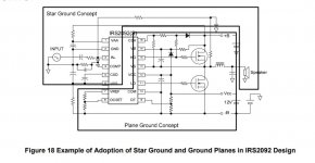
GND on PCB
Let's start with grounding:
APP Note 1139
https://www.infineon.com/dgdl/an-1135.pdf?fileId=5546d462533600a401535599e83610bf
Suggests separating the ground for the input and output, from the the plane of -B (neg rail), using a star grounding principle for GND and Plane for -B.
This can e.g. be found in use in IRAUDAMP5, where the star grounding is more like a GND plane for the input section.
In practice it is not that easy to accomplish, and I have in my designs used the bottom side of a 2 layer board as GND and then routing +B and -B on the topside.
Question is though how much the noisy parts around the output stage will induce of noise and other bad things through the GND plane?
On a 4 layer PCB, you would have the possibility to have a full GND plane, 2 power planes and a routing plane .... question is though if running the GND layer full is at all a good idea in this case also?
Attachments
Specially with single-supplied bridge designs GND is power return as well and contaminated with power noise. For that reason I use a local GND plane for the analog input area that is separated from power GND. It will be connected at one point to AGND-pin of the chip using a smd resistor. Here you can choose everything from zero to 100R. For me this ended up always with zero ohm resistors.
If you dig deeper into distortion measurements you may find unexpected H2 distortion levels. This is a strong indication of magnetic coupling from output current loops to input loops.
For best performance keeps these loops all small as possible.
And keep both current loops around the power blocking caps as SYMMETRICAL as possible for best magnetic field cancellation.
This is by far not academic over-engineering. Keep in mind that THD-levels in the ppm-region are spoiled by input error voltage in the uV-region that can be picked up easily by small magnetic loops.
The output waveform is composed of two halfwaves that must be added perfectly for lowest THD.
Every tiny imbalance produces asymmetric distortion that is associated to H2,H4 etc.
Last edited:
Class D needs very tight decoupling.
Power tracks should be as short and as thick as possible.
I designed a class d amp and sold it on.
Buyer emailed me and said it didn't work.
I asked for a picture of amp and it showed output transistors on 6 inch leads !
He put the transistors back on pcb and it then worked fine.
Class AB rules go out the window with fast class D amplifiers.
@bucks bunny
This is exactly what is suggested by IR. And the small resistor, what I called lifting/isolation resistor is meant to isolate the two ground parts even further. I have also used these, and also ended with 0 ohm. But it is a small component and can be added without much fuss and tried out.
One thing thought I have considered, is whether it would help further to also have separate the GND wires for the input section and the output section, that is to have separate wires going from PSU to the board?? ...... following the argument of keeping them separate on the board sort of leads to this conclusion!
And for the LDOs needed for the input section I would tie their GND to the input GND.
... I need to start doing some measurements of my amps ... never got around to it yet 😉
@nigel, 6 inches! ... he he, yes and with the ever faster MosFets, even the leads on a TO-220 is getting to be a problem
There is no need for separate GND wires to your supply, because the star GND-point is not the supply - but AGND-pin of the amp. Following this ref-GND of LDOs is tied to the same point or to the AGND-input plane respectively. Driving the amps input symmetrically further improves noise immunity.
Last edited:
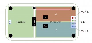
Grounding
Ok to sum it up around Grounding (half bridge):
Keep input and output GND separated.
Maybe use a small resistor e.g. 10 to 100 ohm to separate further.
If using 4 layer PCB, keep GND on one layer, and use a separate layer for power planes, one layer should be sufficient for +B and -B.
Don't run +B/-B planes under or near input section
If using 2 layer, it is more important to keep a plane for -B on the output section (red section on drawing) and then try to obtain best layout for Power GND and +b (thich and short).
If using 4 layer, you could use both top and bottom layer for GND in the input section, thereby screening all routing between.
Attachments
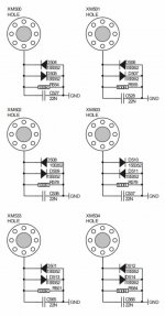
Ground Loop Breakers
Next up is the question of Ground Loop Breakers.
Described here by e.g. Rod Elliott:
Earthing (Grounding) Your Hi-Fi - Tricks and Techniques
An earth loop conducts a current from one piece of equipment to the next, and imposes a voltage across the connection, and the breaker circuit can be used to lower the current between the equipment by mounting a resistor in the path.
If you are using a SMPS, which slowly is becoming the norm also in HiFi, it is maybe not so much the 50 Hz and harmonics, but high freq which poses a problem, and a source for noise.
Checking out the schematics of the NAD M22 (which uses a Hypex SMPS) the amp board is using loop breakers for each mounting hole, but the component choice is not beefy but probably sufficient. See pic.
Any experience in this regard with DIY Class D (or commercial)?
PS. In some countries link DK, power outlets do not normally contain an earth connection ... therefore the chassis will in most cases be floating.
PPS. When you are using a SMPS, input filter is connected to chassis by two small safety caps.
The primary side will be connected to Secondary side by a small cap for EMI reasons.
Attachments
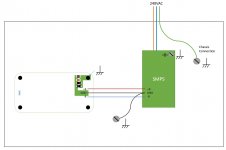
Suggested chassis connection with SMPS and ground loop breakers.
The mains input could of course be further filtered, but in general all SMPS already contain filtering.
The mains input could of course be further filtered, but in general all SMPS already contain filtering.
Attachments
Last edited:
Ok last picture is of course wrong ... either you do the Ground lift on the pcb and thereby connect to the chassis OR you connect GND from the SPU to the chassis 😉
- Home
- Amplifiers
- Class D
- Good design and implementation practice