These are some very interesting parts!
In a sentence, Barrie Gilbert stated that his AFA (active feedback amp) "unlike the OPA (vfb opamp), has high open-loop linearity and excellent closed-loop linearity due to its distortion-canceling topology, and a very high degree of versatility arising from its dual fully-differential inputs, has the potential to eclipse the OPA in all applications involving the manipulation of purely voltage-mode signals."
The purpose of this thread is to get people to try out this topology.
Actual, working designs.
These chips can be used in line-level applications (AD830, LT6552) and head amp/ power amp (TDA856X). abraxalito even said there's one power amp which has a line driver mode selectable by a pin! So I didn't want to put the thread in amp or line level ... 'parts' seemed a good compromise but I hope it gets enough attention ...
Here are some of the chips: AD830, LT6552, TDA856X
(all these are still available)
Let's start with the AD830
AD830 High Speed, Video Difference Amplifier
View attachment AD830.pdf
from the spec sheet:
GENERAL DESCRIPTION
The AD830 is a wideband, differencing amplifier designed for use at video frequencies but also useful in many other applications. It accurately amplifies a fully differential signal at the input and produces an output voltage referred to a user-chosen level. The undesired common-mode signal is rejected, even at high frequencies. High impedance inputs ease interfacing to finite source impedances and, thus, preserve the excellent common-mode rejection. In many respects, it offers significant improvements over discrete difference amplifier approaches, in particular in high frequency common-mode rejection.
ADVANTAGEOUS PROPERTIES OF THE AD830
High common-mode rejection ratio (CMRR)
High impedance inputs
Symmetrical dynamic response for +1 and −1 Gain
Low sensitivity to the value of source R
Equal input impedance for the + and − input
Excellent high frequency CMRR
No halving of the bandwidth
Constant power distortion versus common-mode voltage
Highly matched resistors not needed
UNDERSTANDING THE AD830 TOPOLOGY
The AD830 represents Analog Devices first amplifier product to embody a powerful alternative amplifier topology. Referred to as active feedback, the topology used in the AD830 provides inherent advantages in the handling of differential signals, differing system commons, level shifting, and low distortion, high frequency amplification. In addition, it makes possible the implementation of many functions not realizable with single op amp circuits or superior to op amp based equivalent circuits. With this in mind, it is important to understand the internal structure of the AD830.
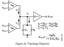
The topology, reduced to its elemental form, is shown in Figure 26.
Nonideal effects, such as nonlinearity, bias currents, and limited full scale, are omitted from this model for simplicity but are discussed later. The key feature of this topology is the use of two, identical voltage-to-current converters, GM, that make up input and feedback signal interfaces. They are labeled with inputs VX and VY, respectively. These voltage-to-current converters possess fully differential inputs, high linearity, high input impedance, and wide voltage range operation. This enables the part to handle large amplitude differential signals; it also provides high common-mode rejection, low distortion, and negligible loading on the source.
The label, GM, is meant to convey that the transconductance is a large signal quantity, unlike in the front end of most op amps. The two GM stage current outputs, IX and IY, sum together at a high impedance node, which is characterized by an equivalent resistance and capacitance connected to an ac common. A unity voltage gain stage follows the high impedance node to provide buffering from loads. Relative to either input, the open-loop gain, AOL, is set by the transconductance, GM, working into the resistance, RP; AOL = GM × RP. The unity gain frequency, ω0 dB, for the open-loop gain is established by the transconductance, GM, working into the capacitance, CC; ω0 dB = GM/CC. The open-loop description of the AD830 is shown below for completeness.
Precise amplification is accomplished through closed-loop operation of this topology. Voltage feedback is implemented via the Y GM stage where the output is connected to the −Y input for negative feedback, as shown in Figure 27.
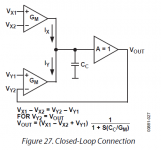
An input signal is applied across the X GM stage, either fully differential or single-ended referred to common. It produces a current signal that is summed at the high impedance node with the output current from the Y GM stage. Negative feedback nulls this sum to a small error current necessary to develop the output voltage at the high impedance node. The error current is usually negligible, so the null condition essentially forces the Y GM output stage current to equal the exact X GM output current. Because the two transconductances are identical, the differential voltage across the Y inputs equals the negative of the differential voltage across the X input; VY = −VX or, more precisely, VY2 − VY1 = VX1 − VX2. This simple relation provides the basis to easily analyze any function possible to synthesize with the AD830, including any feedback situation.
The bandwidth of the circuit is defined by the GM and the capacitor, CC. The highly linear GM stages give the amplifier a single-pole response, excluding the output amplifier and loading effects. It is important to note that the bandwidth and general dynamic behavior is symmetrical (identical) for the noninverting and the inverting connections of the AD830. In addition, the input impedance and CMRR are the same for either connection. This is very advantageous and unlike in a voltage or current feedback amplifier where there is a distinct difference in performance between the inverting and noninverting gain. The practical importance of this cannot be overemphasized and is a key feature offered by the AD830 amplifier topology.
😎
And here are some of the circuits from the spec sheet:
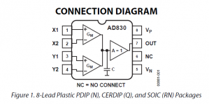
Connection diagram

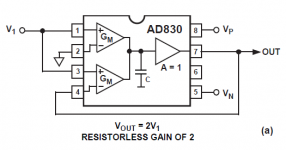
Gain of 2
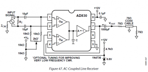
AC coupled line receiver
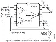
Diff amp level shift
Much of this technical discussion is a bit beyond me so I'm hoping to attract some heavy-hitters to help summarize, explain, apply, and design some actual circuits. Now, if you want someone to poorly implement the design and then wax on about how good it sounds ... well I'm your man! 😉
Anyone have any ideas? Ways to apply these circuits? New circuits that use this topology/chip?
Here's abraxalito with an application:
Opamps tend not to like the high levels of RF coming out of DACs, I recommend passive (LC) filtering before the opamp - OPA627 is one of the better ones at dealing with RF. Better still though an AFA like AD830, this one is highly RF resistant and sounded great when fed with TDA1545.
http://www.diyaudio.com/forums/digit...hematic-3.html
Cheers,
Jeff
P.S. And here are Gilbert's two articles:
Are Opamps Really Linear?
View attachment Are Op Amps Really Linear.pdf
Nonlinear Effects of Radio-Frequency Interference in Opamps
View attachment Nonlinear Effects of Radio-Frequency Interference in Opamps opampsusc_01.pdf
Next up, LT6552 and TDA856X.
P.S.S. Here are some threads referencing the AFA that I'll draw from (if you know of any more, please add them):
http://www.diyaudio.com/forums/solid-state/19690-active-feedback-amplifier.html#post3392351
http://www.diyaudio.com/forums/digital-line-level/225960-ad1865-schematic-3.html
http://www.diyaudio.com/forums/power-supplies/229345-powering-high-end-usb-dac-2.html
http://www.diyaudio.com/forums/blogs/abraxalito/960-high-end-chipamp-build-project.html
Possibly the most frugal high-end sounding amp?
http://www.marchandelec.com/ftp/revpm48.pdf
In a sentence, Barrie Gilbert stated that his AFA (active feedback amp) "unlike the OPA (vfb opamp), has high open-loop linearity and excellent closed-loop linearity due to its distortion-canceling topology, and a very high degree of versatility arising from its dual fully-differential inputs, has the potential to eclipse the OPA in all applications involving the manipulation of purely voltage-mode signals."
The purpose of this thread is to get people to try out this topology.
Actual, working designs.
These chips can be used in line-level applications (AD830, LT6552) and head amp/ power amp (TDA856X). abraxalito even said there's one power amp which has a line driver mode selectable by a pin! So I didn't want to put the thread in amp or line level ... 'parts' seemed a good compromise but I hope it gets enough attention ...
Here are some of the chips: AD830, LT6552, TDA856X
(all these are still available)
Let's start with the AD830
AD830 High Speed, Video Difference Amplifier
View attachment AD830.pdf
from the spec sheet:

GENERAL DESCRIPTION
The AD830 is a wideband, differencing amplifier designed for use at video frequencies but also useful in many other applications. It accurately amplifies a fully differential signal at the input and produces an output voltage referred to a user-chosen level. The undesired common-mode signal is rejected, even at high frequencies. High impedance inputs ease interfacing to finite source impedances and, thus, preserve the excellent common-mode rejection. In many respects, it offers significant improvements over discrete difference amplifier approaches, in particular in high frequency common-mode rejection.
ADVANTAGEOUS PROPERTIES OF THE AD830
High common-mode rejection ratio (CMRR)
High impedance inputs
Symmetrical dynamic response for +1 and −1 Gain
Low sensitivity to the value of source R
Equal input impedance for the + and − input
Excellent high frequency CMRR
No halving of the bandwidth
Constant power distortion versus common-mode voltage
Highly matched resistors not needed
UNDERSTANDING THE AD830 TOPOLOGY
The AD830 represents Analog Devices first amplifier product to embody a powerful alternative amplifier topology. Referred to as active feedback, the topology used in the AD830 provides inherent advantages in the handling of differential signals, differing system commons, level shifting, and low distortion, high frequency amplification. In addition, it makes possible the implementation of many functions not realizable with single op amp circuits or superior to op amp based equivalent circuits. With this in mind, it is important to understand the internal structure of the AD830.

The topology, reduced to its elemental form, is shown in Figure 26.
Nonideal effects, such as nonlinearity, bias currents, and limited full scale, are omitted from this model for simplicity but are discussed later. The key feature of this topology is the use of two, identical voltage-to-current converters, GM, that make up input and feedback signal interfaces. They are labeled with inputs VX and VY, respectively. These voltage-to-current converters possess fully differential inputs, high linearity, high input impedance, and wide voltage range operation. This enables the part to handle large amplitude differential signals; it also provides high common-mode rejection, low distortion, and negligible loading on the source.
The label, GM, is meant to convey that the transconductance is a large signal quantity, unlike in the front end of most op amps. The two GM stage current outputs, IX and IY, sum together at a high impedance node, which is characterized by an equivalent resistance and capacitance connected to an ac common. A unity voltage gain stage follows the high impedance node to provide buffering from loads. Relative to either input, the open-loop gain, AOL, is set by the transconductance, GM, working into the resistance, RP; AOL = GM × RP. The unity gain frequency, ω0 dB, for the open-loop gain is established by the transconductance, GM, working into the capacitance, CC; ω0 dB = GM/CC. The open-loop description of the AD830 is shown below for completeness.
Precise amplification is accomplished through closed-loop operation of this topology. Voltage feedback is implemented via the Y GM stage where the output is connected to the −Y input for negative feedback, as shown in Figure 27.

An input signal is applied across the X GM stage, either fully differential or single-ended referred to common. It produces a current signal that is summed at the high impedance node with the output current from the Y GM stage. Negative feedback nulls this sum to a small error current necessary to develop the output voltage at the high impedance node. The error current is usually negligible, so the null condition essentially forces the Y GM output stage current to equal the exact X GM output current. Because the two transconductances are identical, the differential voltage across the Y inputs equals the negative of the differential voltage across the X input; VY = −VX or, more precisely, VY2 − VY1 = VX1 − VX2. This simple relation provides the basis to easily analyze any function possible to synthesize with the AD830, including any feedback situation.
The bandwidth of the circuit is defined by the GM and the capacitor, CC. The highly linear GM stages give the amplifier a single-pole response, excluding the output amplifier and loading effects. It is important to note that the bandwidth and general dynamic behavior is symmetrical (identical) for the noninverting and the inverting connections of the AD830. In addition, the input impedance and CMRR are the same for either connection. This is very advantageous and unlike in a voltage or current feedback amplifier where there is a distinct difference in performance between the inverting and noninverting gain. The practical importance of this cannot be overemphasized and is a key feature offered by the AD830 amplifier topology.
😎
And here are some of the circuits from the spec sheet:
Connection diagram

Gain of 2

AC coupled line receiver

Diff amp level shift

Much of this technical discussion is a bit beyond me so I'm hoping to attract some heavy-hitters to help summarize, explain, apply, and design some actual circuits. Now, if you want someone to poorly implement the design and then wax on about how good it sounds ... well I'm your man! 😉
Anyone have any ideas? Ways to apply these circuits? New circuits that use this topology/chip?
Here's abraxalito with an application:
Opamps tend not to like the high levels of RF coming out of DACs, I recommend passive (LC) filtering before the opamp - OPA627 is one of the better ones at dealing with RF. Better still though an AFA like AD830, this one is highly RF resistant and sounded great when fed with TDA1545.
http://www.diyaudio.com/forums/digit...hematic-3.html
Cheers,
Jeff
P.S. And here are Gilbert's two articles:
Are Opamps Really Linear?
View attachment Are Op Amps Really Linear.pdf
Nonlinear Effects of Radio-Frequency Interference in Opamps
View attachment Nonlinear Effects of Radio-Frequency Interference in Opamps opampsusc_01.pdf
Next up, LT6552 and TDA856X.
P.S.S. Here are some threads referencing the AFA that I'll draw from (if you know of any more, please add them):
http://www.diyaudio.com/forums/solid-state/19690-active-feedback-amplifier.html#post3392351
http://www.diyaudio.com/forums/digital-line-level/225960-ad1865-schematic-3.html
http://www.diyaudio.com/forums/power-supplies/229345-powering-high-end-usb-dac-2.html
http://www.diyaudio.com/forums/blogs/abraxalito/960-high-end-chipamp-build-project.html
Possibly the most frugal high-end sounding amp?
http://www.marchandelec.com/ftp/revpm48.pdf
Last edited:
A similar chip (but this spec sheet has a simplified schematic!):
View attachment LT6552.pdf
The LT6552 is a video difference amplifier optimized for low voltage single supply operation. This versatile amplifier features uncommitted high input impedance (+) and (–) inputs and can be used in differential or single-ended configurations. A second set of inputs gives gain adjustment and DC control to the differential amplifier.
APPLICATION INFORMATION
The LT6552 is a video difference amplifier with two pairs of high impedance inputs. The primary purpose of the LT6552 is to convert high frequency differential signals into a single-ended output, while rejecting any common mode noise. In the simplest configuration, one pair of inputs is connected to the incoming differential signal, while the other pair of inputs is used to set amplifier gain and DC level. The device will operate on either single or dual supplies and has an input common mode range which includes the negative supply. The common mode rejection ratio is greater than 60dB at 10MHz. Feedback is applied to Pin 8 and the LT6552’s transient response is optimized for gains of 2 or greater.
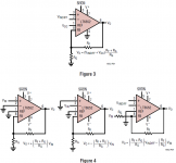
Figure 3 shows the single supply connection. The amplifier gain is set by a feedback network from the output to Pin 8 (FB). A DC signal applied to Pin 1 (REF) establishes the output quiescent voltage and the differential signal is applied to Pins 2 and 3. Figure 4 shows several other connections using dual supplies. In each case, the amplifier gain is set by a feedback network from the output to Pin 8 (FB).
AMPLIFIER CHARACTERISTICS
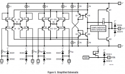
Figure 5 shows a simplified schematic of the LT6552. There are two input stages; the first one consists of transistors Q1 to Q8 for the (+) and (–) inputs while the second input stage consists of transistors Q9 to Q16 for the reference and feedback inputs. This topology provides high slew rates at low supply voltages. The input common mode range extends from ground to typically 1.75V from VCC, and is limited by 2VBE’s plus a saturation voltage of current sources I1-I4. Each input stage drives the degeneration resistors of PNP and NPN current mirrors, Q17 to Q20, that convert the differential signals into a single-ended output. The complementary drive generator supplies current to the output transistors that swing from rail-to-rail.
The current generated through R1 or R2, divided by the capacitor CM, determines the slew rate. Note that this current, and hence the slew rate, are proportional to the magnitude of the input step. The input step equals the output step divided by the closed-loop gain. The highest slew rates are therefore obtained in the lowest gain configurations. The Typical Performance Characteristic Curve of Slew Rate vs Closed-Loop Gain shows the details.
...
SHDN Pin (shutdown)
The LT6552 includes a shutdown feature that disables the part, reducing quiescent current and making the output high impedance. The part can be shutdown by bringing the SHDN pin within 0.5V of V–. When shutdown the supply current is typically 400mA and the output leakage current is 0.25mA (V– £ VOUT £ V+). In normal operation the SHDN can be tied to V+ or left floating; if the pin is left unconnected, an internal FET pull-up will keep the LT6552 fully operational.
😎
Same thing here, anyone have any ideas? Ways to apply these circuits? New circuits that use this topology/chip?
Cheers,
Jeff
View attachment LT6552.pdf
The LT6552 is a video difference amplifier optimized for low voltage single supply operation. This versatile amplifier features uncommitted high input impedance (+) and (–) inputs and can be used in differential or single-ended configurations. A second set of inputs gives gain adjustment and DC control to the differential amplifier.
APPLICATION INFORMATION
The LT6552 is a video difference amplifier with two pairs of high impedance inputs. The primary purpose of the LT6552 is to convert high frequency differential signals into a single-ended output, while rejecting any common mode noise. In the simplest configuration, one pair of inputs is connected to the incoming differential signal, while the other pair of inputs is used to set amplifier gain and DC level. The device will operate on either single or dual supplies and has an input common mode range which includes the negative supply. The common mode rejection ratio is greater than 60dB at 10MHz. Feedback is applied to Pin 8 and the LT6552’s transient response is optimized for gains of 2 or greater.

Figure 3 shows the single supply connection. The amplifier gain is set by a feedback network from the output to Pin 8 (FB). A DC signal applied to Pin 1 (REF) establishes the output quiescent voltage and the differential signal is applied to Pins 2 and 3. Figure 4 shows several other connections using dual supplies. In each case, the amplifier gain is set by a feedback network from the output to Pin 8 (FB).
AMPLIFIER CHARACTERISTICS

Figure 5 shows a simplified schematic of the LT6552. There are two input stages; the first one consists of transistors Q1 to Q8 for the (+) and (–) inputs while the second input stage consists of transistors Q9 to Q16 for the reference and feedback inputs. This topology provides high slew rates at low supply voltages. The input common mode range extends from ground to typically 1.75V from VCC, and is limited by 2VBE’s plus a saturation voltage of current sources I1-I4. Each input stage drives the degeneration resistors of PNP and NPN current mirrors, Q17 to Q20, that convert the differential signals into a single-ended output. The complementary drive generator supplies current to the output transistors that swing from rail-to-rail.
The current generated through R1 or R2, divided by the capacitor CM, determines the slew rate. Note that this current, and hence the slew rate, are proportional to the magnitude of the input step. The input step equals the output step divided by the closed-loop gain. The highest slew rates are therefore obtained in the lowest gain configurations. The Typical Performance Characteristic Curve of Slew Rate vs Closed-Loop Gain shows the details.
...
SHDN Pin (shutdown)
The LT6552 includes a shutdown feature that disables the part, reducing quiescent current and making the output high impedance. The part can be shutdown by bringing the SHDN pin within 0.5V of V–. When shutdown the supply current is typically 400mA and the output leakage current is 0.25mA (V– £ VOUT £ V+). In normal operation the SHDN can be tied to V+ or left floating; if the pin is left unconnected, an internal FET pull-up will keep the LT6552 fully operational.
😎
Same thing here, anyone have any ideas? Ways to apply these circuits? New circuits that use this topology/chip?
Cheers,
Jeff
Last edited:
Next is the TDA856x
Here's the selection chart:
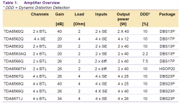
What is DDD?
DDD = Dynamic Distortion Detection
(From TDA8561Q datasheet, we'll see later)
Diagnostic output (pin 16)
DYNAMIC DISTORTION DETECTOR (DDD)
At the onset of clipping of one or more output stages, the dynamic distortion detector becomes active and pin 16 goes LOW. This information can be used to drive a sound processor or DC volume control to attenuate the input signal and thus limit the distortion. The output level of pin 16 is independent of the number of channels that are clipping (see Figs 3 and 4).
View attachment TDA856x selection AN10327.pdf
abraxalito is playing with the TDA8561 but also references the TDA8566 because it's still available at Mouser.
View attachment TDA8566.pdf
General description
The TDA8566 is an integrated class-B output amplifier which is available in several packages. TDA8566TH is contained in a 20-lead small outline plastic package. The TDA8566TH1 is a 24-lead small outline plastic package which is pin compatible with the I2C-bus controlled amplifier TDA1566TH for one board layout. TDA8566Q is a 17-pin DIL-bent-SIL package.
The device contains 2 amplifiers in a Bridge-Tied Load (BTL) configuration. The output power is 2 ´ 25 W in a 4 W load or 2 ´ 40 W in a 2 W load. It has a differential input stage and 2 diagnostic outputs. The device is primarily developed for car radio applications.
Features
Differential inputs
Very high Common Mode Rejection Ratio (CMRR)
High common mode input signal handling
Requires very few external components
High output power
4 W and 2 W load driving capability
Low offset voltage at output
Fixed gain
Diagnostic facility (distortion, short-circuit and temperature pre-warning)
Good ripple rejection
Mode select switch (operating, mute and standby)
Load dump protection
Short-circuit proof to ground, to VP and across the load
Low power dissipation in any short-circuit condition
Thermally protected
Reverse polarity safe
Protected against electrostatic discharge
No switch-on/switch-off plops
Low thermal resistance
TDA8566TH1 is pin compatible with TDA1566TH
...
The TDA8566 contains 2 identical amplifiers and can be used for BTL applications. The gain of each amplifier is fixed at 26 dB. Special features of this device are:
Mode select switch
Clip detection
Short-circuit diagnostic
Temperature pre-warning
Open-collector diagnostic outputs
Differential inputs
...
Mode select switch (pin MODE)
Standby: low supply current
Mute: input signal suppressed
Operating: normal on condition
Since this pin has a very low input current (< 40 mA), a low-cost supply switch can be applied. To avoid switch-on plops, it is advisable to keep the amplifier in the mute mode for a period of ³ 150 ms (charging the input capacitors at pins IN1+, IN1-, IN2+ and IN2-). This can be realized by using a microcontroller or by using an external timing circuit as illustrated in Figure 8.
...
Clip detection (pin CLIP)
When clipping occurs at one or more output stages, the dynamic distortion detector becomes active and pin CLIP goes LOW. This information can be used to drive a sound processor or a DC volume control to attenuate the input signal and so limit the level of distortion. The output level of pin CLIP is independent of the number of channels that are being clipped. The clip detection circuit is disabled in a short-circuit condition, so if a fault condition occurs at the outputs, pin CLIP will remain at a HIGH level. The clip detection waveforms are illustrated in Figure 5.
...
Temperature pre-warning (pin DIAG)
When the virtual junction temperature (Tvj) reaches 145 °C, pin DIAG will become continuously LOW.
...
😎
Here's the Block Diagram
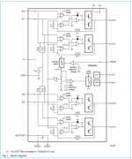
And a stereo BTL circuit
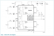
As mentioned, abraxalito is playing with the TDA8561:
http://www.diyaudio.com/forums/blogs/abraxalito/960-high-end-chipamp-build-project.html
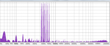
Here are the first measurements - the Nitro amp being fed by the Ozone DAC with a six-tone multiple, peak digital level -20dB. Peak output power around 100mW in an 8R speaker (connected for this test). It looks from this that the datasheet is a little pessimistic on THD, though here I'm measuring the TDA8566, not the 8561. No measurement graphs are presented in the 8566 DS and the 8561 only has plots for 2R and 4R loads, not 8R.
The TDA8561 schematic
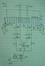
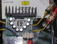
Actual circuit!
And the mods for the TDA8566 (at Mouser)
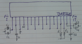
Additional schematic showing how to use TDA8566Q in place of TDA8561Q as the latter isn't available from Mouser. Mouser only has fewer than 300 TDA8566Q in stock so best to get in quick - I doubt they'll be getting more as this chip is going obsolete. The pins shown unconnected in the mod schematic aren't unconnected - it means they're connected the same way as for the TDA8561Q.
Here's some of the reasoning behind the choice of the TDA856x from abraxalito (opus11):
Possibly the most frugal high-end sounding amp?
Having built chipamp based amps for a number of years, they produce great but not stellar sound in the main, when issues like grounding and decoupling are addressed fully. I have the hypothesis that what holds them back is the input stage, being as it is typically a LTP and a bipolar one at that. Added to that, they do tend to have inadequate PSRR by virtue of not having power supply separation between the signal and output stages. So they pollute their own patch, so to speak and filters can't be included because the necessary wires aren't brought off-chip.
I have up until fairly recently, played with the TDA7293 because its fairly unique in allowing separation between the voltage and current amplifying stages, especially so when the amplification function is split between two chips. This device is the only one I know of that permits that so the power supply issue can be fully fixed. It does however still have the ubiquitous LTP input stage which has given me so many problems in opamps in terms of excluding HF interference.
The search for a chipamp sans LTP has been running for a few weeks now and recently I've come upon some very interesting parts from Philips - the TDA856X series
Just focusing on the lack of LTP rather than AFA topology ...
Here's the selection chart:

What is DDD?
DDD = Dynamic Distortion Detection
(From TDA8561Q datasheet, we'll see later)
Diagnostic output (pin 16)
DYNAMIC DISTORTION DETECTOR (DDD)
At the onset of clipping of one or more output stages, the dynamic distortion detector becomes active and pin 16 goes LOW. This information can be used to drive a sound processor or DC volume control to attenuate the input signal and thus limit the distortion. The output level of pin 16 is independent of the number of channels that are clipping (see Figs 3 and 4).
View attachment TDA856x selection AN10327.pdf
abraxalito is playing with the TDA8561 but also references the TDA8566 because it's still available at Mouser.
View attachment TDA8566.pdf
General description
The TDA8566 is an integrated class-B output amplifier which is available in several packages. TDA8566TH is contained in a 20-lead small outline plastic package. The TDA8566TH1 is a 24-lead small outline plastic package which is pin compatible with the I2C-bus controlled amplifier TDA1566TH for one board layout. TDA8566Q is a 17-pin DIL-bent-SIL package.
The device contains 2 amplifiers in a Bridge-Tied Load (BTL) configuration. The output power is 2 ´ 25 W in a 4 W load or 2 ´ 40 W in a 2 W load. It has a differential input stage and 2 diagnostic outputs. The device is primarily developed for car radio applications.
Features
Differential inputs
Very high Common Mode Rejection Ratio (CMRR)
High common mode input signal handling
Requires very few external components
High output power
4 W and 2 W load driving capability
Low offset voltage at output
Fixed gain
Diagnostic facility (distortion, short-circuit and temperature pre-warning)
Good ripple rejection
Mode select switch (operating, mute and standby)
Load dump protection
Short-circuit proof to ground, to VP and across the load
Low power dissipation in any short-circuit condition
Thermally protected
Reverse polarity safe
Protected against electrostatic discharge
No switch-on/switch-off plops
Low thermal resistance
TDA8566TH1 is pin compatible with TDA1566TH
...
The TDA8566 contains 2 identical amplifiers and can be used for BTL applications. The gain of each amplifier is fixed at 26 dB. Special features of this device are:
Mode select switch
Clip detection
Short-circuit diagnostic
Temperature pre-warning
Open-collector diagnostic outputs
Differential inputs
...
Mode select switch (pin MODE)
Standby: low supply current
Mute: input signal suppressed
Operating: normal on condition
Since this pin has a very low input current (< 40 mA), a low-cost supply switch can be applied. To avoid switch-on plops, it is advisable to keep the amplifier in the mute mode for a period of ³ 150 ms (charging the input capacitors at pins IN1+, IN1-, IN2+ and IN2-). This can be realized by using a microcontroller or by using an external timing circuit as illustrated in Figure 8.
...
Clip detection (pin CLIP)
When clipping occurs at one or more output stages, the dynamic distortion detector becomes active and pin CLIP goes LOW. This information can be used to drive a sound processor or a DC volume control to attenuate the input signal and so limit the level of distortion. The output level of pin CLIP is independent of the number of channels that are being clipped. The clip detection circuit is disabled in a short-circuit condition, so if a fault condition occurs at the outputs, pin CLIP will remain at a HIGH level. The clip detection waveforms are illustrated in Figure 5.
...
Temperature pre-warning (pin DIAG)
When the virtual junction temperature (Tvj) reaches 145 °C, pin DIAG will become continuously LOW.
...
😎
Here's the Block Diagram

And a stereo BTL circuit

As mentioned, abraxalito is playing with the TDA8561:
http://www.diyaudio.com/forums/blogs/abraxalito/960-high-end-chipamp-build-project.html
Here are the first measurements - the Nitro amp being fed by the Ozone DAC with a six-tone multiple, peak digital level -20dB. Peak output power around 100mW in an 8R speaker (connected for this test). It looks from this that the datasheet is a little pessimistic on THD, though here I'm measuring the TDA8566, not the 8561. No measurement graphs are presented in the 8566 DS and the 8561 only has plots for 2R and 4R loads, not 8R.

The TDA8561 schematic

Actual circuit!

And the mods for the TDA8566 (at Mouser)

Additional schematic showing how to use TDA8566Q in place of TDA8561Q as the latter isn't available from Mouser. Mouser only has fewer than 300 TDA8566Q in stock so best to get in quick - I doubt they'll be getting more as this chip is going obsolete. The pins shown unconnected in the mod schematic aren't unconnected - it means they're connected the same way as for the TDA8561Q.
Here's some of the reasoning behind the choice of the TDA856x from abraxalito (opus11):
Possibly the most frugal high-end sounding amp?
Having built chipamp based amps for a number of years, they produce great but not stellar sound in the main, when issues like grounding and decoupling are addressed fully. I have the hypothesis that what holds them back is the input stage, being as it is typically a LTP and a bipolar one at that. Added to that, they do tend to have inadequate PSRR by virtue of not having power supply separation between the signal and output stages. So they pollute their own patch, so to speak and filters can't be included because the necessary wires aren't brought off-chip.
I have up until fairly recently, played with the TDA7293 because its fairly unique in allowing separation between the voltage and current amplifying stages, especially so when the amplification function is split between two chips. This device is the only one I know of that permits that so the power supply issue can be fully fixed. It does however still have the ubiquitous LTP input stage which has given me so many problems in opamps in terms of excluding HF interference.
The search for a chipamp sans LTP has been running for a few weeks now and recently I've come upon some very interesting parts from Philips - the TDA856X series
Just focusing on the lack of LTP rather than AFA topology ...
Last edited:
Gilbert's chips, AFA (active feedback amplifier): AD8129, AD8130
Knew I'd miss one!
View attachment AD8129 AD8130.pdf
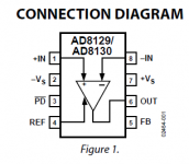
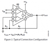
THEORY OF OPERATION
The AD8129/AD8130 use an architecture called active feedback, which differs from that of conventional op amps. The most obvious differentiating feature is the presence of two separate pairs of differential inputs compared with a conventional op amp’s single pair. Typically, for the active feedback architecture, one of these input pairs is driven by a differential input signal, while the other is used for the feedback. This active stage in the feedback path is where the term active feedback is derived.
The active feedback architecture offers several advantages over a conventional op amp in many types of applications. Among these are excellent common-mode rejection, wide input common-mode range, and a pair of inputs that are high impedance and completely balanced in a typical application. In addition, while an external feedback network establishes the gain response as in a conventional op amp, its separate path makes it completely independent of the signal input. This eliminates any interaction between the feedback and input circuits, which traditionally causes problems with CMRR in conventional differential-input op amp circuits.
Another advantage is the ability to change the polarity of the gain merely by switching the differential inputs. A high input-impedance inverting amplifier can be made. Besides a high input impedance, a unity-gain inverter with the AD8130 has a noise gain of unity. This produces lower output noise and higher bandwidth than op amps that have noise gain equal to 2 for a unity-gain inverter.
The two differential input stages of the AD8129/AD8130 are each transconductance stages that are well matched. These stages convert the respective differential input voltages to internal currents. The currents are then summed and converted to a voltage, which is buffered to drive the output. The compensation capacitor is in the summing circuit.
When the feedback path is closed around the part, the output drives the feedback input to the voltage that causes the internal currents to sum to 0. This occurs when the two differential inputs are equal and opposite; that is, their algebraic sum is 0.
In a closed-loop application, a conventional op amp has its differential input voltage driven to near 0 under nontransient conditions. The AD8129/AD8130 generally has differential input voltages at each of its input pairs, even under equilibrium conditions. As a practical consideration, it is necessary to limit the differential input voltage internally with a clamp circuit.
Therefore, the input dynamic ranges are limited to about 2.5 V for the AD8130 and 0.5 V for the AD8129 (see the AD8129/AD8130 Specifications section for more detail). For this and other reasons, it is not recommended to reverse the input and feedback stages of the AD8129/AD8130, even though some apparently normal functionality may be observed under some conditions. A few simple circuits can illustrate how the active feedback architecture of the AD8129/AD8130 operates.
Knew I'd miss one!
View attachment AD8129 AD8130.pdf


THEORY OF OPERATION
The AD8129/AD8130 use an architecture called active feedback, which differs from that of conventional op amps. The most obvious differentiating feature is the presence of two separate pairs of differential inputs compared with a conventional op amp’s single pair. Typically, for the active feedback architecture, one of these input pairs is driven by a differential input signal, while the other is used for the feedback. This active stage in the feedback path is where the term active feedback is derived.
The active feedback architecture offers several advantages over a conventional op amp in many types of applications. Among these are excellent common-mode rejection, wide input common-mode range, and a pair of inputs that are high impedance and completely balanced in a typical application. In addition, while an external feedback network establishes the gain response as in a conventional op amp, its separate path makes it completely independent of the signal input. This eliminates any interaction between the feedback and input circuits, which traditionally causes problems with CMRR in conventional differential-input op amp circuits.
Another advantage is the ability to change the polarity of the gain merely by switching the differential inputs. A high input-impedance inverting amplifier can be made. Besides a high input impedance, a unity-gain inverter with the AD8130 has a noise gain of unity. This produces lower output noise and higher bandwidth than op amps that have noise gain equal to 2 for a unity-gain inverter.
The two differential input stages of the AD8129/AD8130 are each transconductance stages that are well matched. These stages convert the respective differential input voltages to internal currents. The currents are then summed and converted to a voltage, which is buffered to drive the output. The compensation capacitor is in the summing circuit.
When the feedback path is closed around the part, the output drives the feedback input to the voltage that causes the internal currents to sum to 0. This occurs when the two differential inputs are equal and opposite; that is, their algebraic sum is 0.
In a closed-loop application, a conventional op amp has its differential input voltage driven to near 0 under nontransient conditions. The AD8129/AD8130 generally has differential input voltages at each of its input pairs, even under equilibrium conditions. As a practical consideration, it is necessary to limit the differential input voltage internally with a clamp circuit.
Therefore, the input dynamic ranges are limited to about 2.5 V for the AD8130 and 0.5 V for the AD8129 (see the AD8129/AD8130 Specifications section for more detail). For this and other reasons, it is not recommended to reverse the input and feedback stages of the AD8129/AD8130, even though some apparently normal functionality may be observed under some conditions. A few simple circuits can illustrate how the active feedback architecture of the AD8129/AD8130 operates.
Gilbert's Pin, AD844 pin5 TZ
While not an AFA chip, this one I'll call:
Gilbert's Pin, AD844 pin5 TZ
From an old thread (2004!) with ... Holy Heavy Hitters Batman! Charles Hansen, John Curl, Walt Jung, ... and the old gang! Jocko, PMA, CarlosFM, Pedja, Elso 😱
DIYHiFi.org • View topic - "Op-amps unsuitable for audio DAC I/V" - myth?
View attachment AD844.pdf
AD844 simplified schematic:
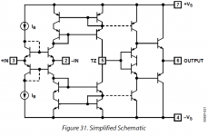
CG describes the issue:
"The AD844 is a special case. It's a current feedback type amplifier. The transimpedance node is connected to a pin on the package, which allows the part to be used open loop (actually, as the AD797 can be) if you want to run it that way. There may be good reasons to do so... Thank Barrie Gilbert for following Wyn Palmer's lead on making this pin available. (Wyn was a serious DIY audio guy at one time.) ..."
Gilbert's Pin! 😉
CG continues with some great description:
"Back to the AD844 thing for those who didn't read the previous thread. Or threads.
The AD844, like the AD846 before it, use a classic CFB topology. The non-inverting input is a complementary pair of bipolar devices driven at their bases. The collectors are connected to current mirrors that ultimately connect to the Tz node. This Tz node is available at one of the pins. From the Tz node to the output is a complementary buffer stage. Or stages. The inverting input is at the connection of the emitters for the complementary input devices. It's shown in the data sheet.
So... If you connect the inverting input to ground through a resistor and add a resistor to ground from the Tz pin, you can build a pretty nice open loop amplifier. The devices inside are nicely matched because of the IC fabrication process. You can use the buffer as is or add your own externally..."

Georgehifi has been trying the AD844 in this exotic configuration with his PCM1704
http://www.diyaudio.com/forums/digital-source/227677-using-ad844-i-v-14.html
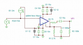
and I'm about to try it with my TDA1541 using Pedja's old circuit
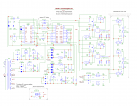
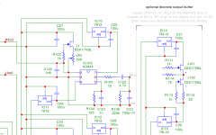
While not an AFA chip, this one I'll call:
Gilbert's Pin, AD844 pin5 TZ
From an old thread (2004!) with ... Holy Heavy Hitters Batman! Charles Hansen, John Curl, Walt Jung, ... and the old gang! Jocko, PMA, CarlosFM, Pedja, Elso 😱
DIYHiFi.org • View topic - "Op-amps unsuitable for audio DAC I/V" - myth?
View attachment AD844.pdf
AD844 simplified schematic:

CG describes the issue:
"The AD844 is a special case. It's a current feedback type amplifier. The transimpedance node is connected to a pin on the package, which allows the part to be used open loop (actually, as the AD797 can be) if you want to run it that way. There may be good reasons to do so... Thank Barrie Gilbert for following Wyn Palmer's lead on making this pin available. (Wyn was a serious DIY audio guy at one time.) ..."
Gilbert's Pin! 😉
CG continues with some great description:
"Back to the AD844 thing for those who didn't read the previous thread. Or threads.
The AD844, like the AD846 before it, use a classic CFB topology. The non-inverting input is a complementary pair of bipolar devices driven at their bases. The collectors are connected to current mirrors that ultimately connect to the Tz node. This Tz node is available at one of the pins. From the Tz node to the output is a complementary buffer stage. Or stages. The inverting input is at the connection of the emitters for the complementary input devices. It's shown in the data sheet.
So... If you connect the inverting input to ground through a resistor and add a resistor to ground from the Tz pin, you can build a pretty nice open loop amplifier. The devices inside are nicely matched because of the IC fabrication process. You can use the buffer as is or add your own externally..."

Georgehifi has been trying the AD844 in this exotic configuration with his PCM1704
http://www.diyaudio.com/forums/digital-source/227677-using-ad844-i-v-14.html

and I'm about to try it with my TDA1541 using Pedja's old circuit


Last edited:
I agree that the AD844 is a very interesting chip. I used it in my error correction power amp as published by Elektor and AudioXpress. Basically, when you run it open loop with a load at the Tz node, you can have a defined gain with no loop feedback.
As to the AD830 and company, I believe that history shows us that Barrie's enthousiasm was not universially appreciated, to be diplomatic.
Maybe that is because it really is not THAT linear - you always need a certain voltage difference on the input pins and those input stages are not very linear.
At one point when I was in contact with Barrie, I asked for a super-duper AD844 successor. He answered that they had one 'on the shelf' but that demand probably would not be high enough to take it in production.
Don't you wish you had a $1M to spare to spend on IC's 😉
jan
Yes.Don't you wish you had a $1M to spare to spend on IC's 😉
jan
...As to the AD830 and company, I believe that history shows us that Barrie's enthousiasm was not universially appreciated, to be diplomatic.
Maybe that is because it really is not THAT linear - you always need a certain voltage difference on the input pins and those input stages are not very linear..
.
This is true, however as abraxalito points out they may be linear enough (diminishing returns) and they shine where many conventional topologies start to stumble--high freq performance, in our cellular/wifi world.
abraxalito
http://www.diyaudio.com/forums/blogs/abraxalito/960-high-end-chipamp-build-project.html
"...the concept I am running hard here with is noise modulation. When I have a hypothesis I try my damndest to break it, flog it to death, test it in many ways to see how strong it is. This is one such test of the 'noise modulation is the missing SQ metric' hypothesis. So the high THD of this chip works in my favour.
...
THD is the metric that Scott's using, he, like Doug Self pays little or no attention to what (IME) really matters for SQ which is low level IMD performance. So you're of the school that -100dB THD is a non-negotiable requirement for high-end sound? If so then there are a whole lot of high-end amps (considered subjectively) which violate that by huge margins!"
Jan, can you say more about your AD844 circuit?
Well, the '844 circuit in isolation is simple - but it is embedded in an output stage (and there is also a Vas stage) error correction scheme.
jan
jan
This is true, however as abraxalito points out they may be linear enough (diminishing returns) and they shine where many conventional topologies start to stumble--high freq performance, in our cellular/wifi world.
Agreed, but one important factor here is 'we've done it always like this'. One design engineer once told me they HAD to call the '844 an 'opamp', otherwise nobody would buy it.
People buy opamps and not some other fancy-named contraption that they have no idea what it does, even if it would fit perfectly in their project.
jan
As to the AD830 and company, I believe that history shows us that Barrie's enthousiasm was not universially appreciated, to be diplomatic.
Maybe that is because it really is not THAT linear - you always need a certain voltage difference on the input pins and those input stages are not very linear.
jan
Jan you are quite correct, in practice the matching of the two halves of the AFA has limitations and these parts specified for reasonable yield rarely did better than .05 to .1% or 60-70 dBc. The AD844 is an op-amp BTW.
Current SOTA is -80dBc THD at 500MHz for amps at this time.
ALD - Please elaborate on what you mean by low level IMD in the absence of THD producing mechanisms.
Last edited:
That's very impressive 😀Current SOTA is -80dBc THD at 500MHz for amps at this time.
Jan you are quite correct, in practice the matching of the two halves of the AFA has limitations and these parts specified for reasonable yield rarely did better than .05 to .1% or 60-70 dBc...
Can you say more?
...
ALD - Please elaborate on what you mean by low level IMD in the absence of THD producing mechanisms.
I was pulling quotes off of abraxalito's blog:
http://www.diyaudio.com/forums/blogs/abraxalito/960-high-end-chipamp-build-project.html
abraxalito makes a high end chipamp from the TDA8561Q
Frank comments that "the THD figures are an order of magnitude worse than for the National chips, and the PSRR looks pretty dismal"
ab: "...the concept I am running hard here with is noise modulation. When I have a hypothesis I try my damndest to break it, flog it to death, test it in many ways to see how strong it is. This is one such test of the 'noise modulation is the missing SQ metric' hypothesis. So the high THD of this chip works in my favour..."
Frank: "I've used LTspice to look at Scott Wurcer's new baby, the Discrete Opamp, and Bob Cordell's "final", high performance power amp from his book. That's the order of performance I was getting, and what I'm looking for personally, as a safety margin..."
ab: "Order of performance for what? THD is the metric that Scott's using, he, like Doug Self pays little or no attention to what (IME) really matters for SQ which is low level IMD performance. So you're of the school that -100dB THD is a non-negotiable requirement for high-end sound? If so then there are a whole lot of high-end amps (considered subjectively) which violate that by huge margins! ..."
They go on to talk about PSRR, LM3886 and powersupplies, then:
ab:
"I agree that the power supply is the big issue, but only once the lower hanging fruit of the architecture (LTP or not LTP) has been plucked. That's low hanging because its easy to fix by just picking the right chip. Once the opamp is blameless then the next layer of that delicious yet eye-watering onion beckons... "
More can be found on his other write up:
Possibly the most frugal high-end sounding amp?
About chipamps he states:
ab: "...I have the hypothesis that what holds them back is the input stage, being as it is typically a LTP and a bipolar one at that. Added to that, they do tend to have inadequate PSRR by virtue of not having power supply separation between the signal and output stages. So they pollute their own patch, so to speak and filters can't be included because the necessary wires aren't brought off-chip...
...The search for a chipamp sans LTP has been running for a few weeks now and recently I've come upon some very interesting parts from Philips - the TDA856X series."
He then references Gilbert's two articles (Are Opamps Really Linear? and Nonlinear Effects of Radio-Frequency Interference in Opamps) and:
"The second paper is much more recent and covers real-world issues with LTPs in opamps which Barrie Gilbert doesn't address, maybe he wasn't even aware of. These issues have probably only come to light because of the greater degree of electromagnetic pollution in today's world - we live bathed in GSM and WiFi signals."
View attachment Nonlinear Effects of Radio-Frequency Interference in Opamps opampsusc_01.pdf
He then notes Charles Hansen's review of the PM48 (TDA8566, AFA chip)
http://www.marchandelec.com/ftp/revpm48.pdf
Talking about including the LTP in the feedback:
ab: "As to why they'd leave the LTP out of the loop - I think its perhaps because they haven't realized it is out of the loop. If they have realized then probably they think that its only an issue at DC - because offset is the only thing out of the loop - and haven't understood that RF is varying the offset voltage. Or that they think RF isn't an issue at audio. Just my speculation! "
He then goes on to do some power supply testing ...
abraxalito said he would stop in at this thread ...
Last edited:
Yep I'm still reading - interesting to hear myself quoted back again 🙂
Scott I'm not sure that your question is formulated in a manner I can respond to - of course the low level IMD won't be in the absence of THD producing mechanisms. However having linearity at high level (which is used for THD metric) isn't necessarily going to indicate excellent linearity at lower level (here I'm meaning below -30dB) because there can be a narrow dead band at zero without much effect on the full scale THD - an undithered quantizer at 16bits for example doesn't show up very well on a full-scale THD measurement.
Scott I'm not sure that your question is formulated in a manner I can respond to - of course the low level IMD won't be in the absence of THD producing mechanisms. However having linearity at high level (which is used for THD metric) isn't necessarily going to indicate excellent linearity at lower level (here I'm meaning below -30dB) because there can be a narrow dead band at zero without much effect on the full scale THD - an undithered quantizer at 16bits for example doesn't show up very well on a full-scale THD measurement.
Yep I'm still reading - interesting to hear myself quoted back again 🙂
Scott I'm not sure that your question is formulated in a manner I can respond to - of course the low level IMD won't be in the absence of THD producing mechanisms. However having linearity at high level (which is used for THD metric) isn't necessarily going to indicate excellent linearity at lower level (here I'm meaning below -30dB) because there can be a narrow dead band at zero without much effect on the full scale THD - an undithered quantizer at 16bits for example doesn't show up very well on a full-scale THD measurement.
A dead zone makes low level THD as well as IMD. By their nature classic differential input stages have no dead zone and the high level THD test is a decent metric to verify transfer linearity and slew performance. At least in my case the output stage for the specified load (600 Ohms) has a smooth transfer function around 0. The distortion performance is fine at -30dB.
Barrie Gilbert was concerned with factors that are inherent in the classic op-amp circuit. EMI, RFI, and power supply noise are decoupled in that they can yield to other better design techniques. In some cases circuits with virtually no PSRR can be made to work well. Maybe some folks are prepared to throw in the towel but I would propose that these issues can be dealt with outside of the choice of circuit architecture. That RF induced offset article injects RF directly into the input via a bias tee, hardly the situation in real applications. After all a lot of low level analog circuitry is working quite well (cap touch, audio, mems accelerometer) while your cell phone is blasting RF.
Last edited:
Maybe some folks are prepared to throw in the towel but I would propose that these issues can be dealt with outside of the choice of circuit architecture.
I have thrown in the towel as regards getting the SQ I'm looking for out of opamps and chipamps with LTP inputs. The TDA8566 is currently doing very nicely though so I'll be sticking with AFAs for the forseeable future.
That RF induced offset article injects RF directly into the input via a bias tee, hardly the situation in real applications. After all a lot of low level analog circuitry is working quite well (cap touch, audio, mems accelerometer) while your cell phone is blasting RF.
Is ADI going to follow in TI's footsteps and publish EMIRR reports on opamps? If so I'll be most curious to see the report on the AD797.
Can you say more?
For instance think about trying to track two things that have 10% open-loop linearity to better than say 1%, this would be .1% net mis-match. These circuits are pretty old BTW, the early instrumentation amplifiers relied on open-loop current transfer which is related to AFB. They also suffered from this problem. Check Note 2 below...
http://www.analog.com/static/imported-files/data_sheets/AD521.pdf
Let's not forget AD603 and AD605
AD603 and AD605 are also parts based on AFAs, though these have front-end attenuators which provide a volume control function. I have been using AD605 for well over a year now as I/V amplifier after passive I/V because it conveniently includes this volume stage, giving 40dB or so range of DC voltage controlled volume. It is though susceptible to RF and can't be directly connected to the I/V resistor of a TDA1545 without passive filtering in between if SQ is a priority. With the right filtering though it sounds awesome. Since its power supply is limited to 5.5V its best used to create a balanced output - this also will tend to cancel its high-ish 2H distortion at higher levels. Running balanced also keeps the noise down, which also is a bit marginal single-ended for a 16bit DAC application. I prefer to use it with a 50R source impedance - above this its getting a little noisy for my tastes though 100R is still quite usable in balanced.
http://www.analog.com/static/imported-files/data_sheets/AD605.pdf
AD603 and AD605 are also parts based on AFAs, though these have front-end attenuators which provide a volume control function. I have been using AD605 for well over a year now as I/V amplifier after passive I/V because it conveniently includes this volume stage, giving 40dB or so range of DC voltage controlled volume.
Bushnel used it in one of their golf range finders.🙂
- Home
- Design & Build
- Parts
- Gilbert's chips, AFA (active feedback amplifier): AD830, LT6552, TDA856X