OK, I wasn't sure where best to post this so hopefully I'm in the right spot.
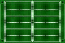
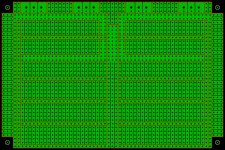
I'm looking to develop a generic prototyping board. I have used several different ones easily available and they so far have been a poor compromise then trying to build a prototype an audio circuit. I'm looking for some input on the design or features to incorporate. Ideally I believe it should be single sided without any plated through holes and lots of opportunity to jumper to power traces and other busses. Any suggestions welcome. I'd like to have a board house make a bunch to make doing prototyping work a little easier. Below is where I'm starting out at. One immediate thought would be to make a couple areas with SMD pads for those who might like to mix technologies.
Anyhow, lend your thoughts or experiences with prototyping boards to help me make this one worth sending out for. Thanks.
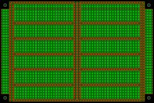
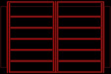
Attachments

Why don't you want plated through holes? I can see if you going to tape and edge at home, you use one side board. But if you sent it out, two sided with plated through holes is going to be more versatile and rugged.
I assume you are doing SS amp. I would actually design in the LTP IPS, the darlington VAS and 4 pairs OPS. Layout the most thorough circuit with all the bells and whistles. Then you can jumper to bypass. I would even do the complementary LTP and you can just not propagate one of them. Look over the SS amp book by Bob Cordell, he really overkill with the design. Put as much of his circuit in and you can always jumper them out.
For tubes, I would use circuit strips to do point to point wiring.
I think you missed my intent. It's for prototyping. I want the boards to be easy to remove components and cheap. With PTH I'm into an automatic two sided process and parts installed are hard to remove without destroying the part or damaging the board. I'm not looking to pin down a specific design or even design elements. If I wanted to just do a specific amp design I would just do a board dedicated to it, and yes with 'options'.
Basically I want to make a blank slate that has bipolar supplies in mind such that it suits audio hobbiests. I think though I should make one long edge better suited to power devices.
Basically I want to make a blank slate that has bipolar supplies in mind such that it suits audio hobbiests. I think though I should make one long edge better suited to power devices.
I've used different types of prototyping boards and can't say I've found one well suited to the audio enthusiast, but yes, conceptually like those but specific to the hobby.
Last edited:
Audio is just another field of electronics, analogue and digital so why cant prototype boards for electronics work for audio!
scraped together some of my previous posts:
I encourage people new to electronics to learn point-to-point prototyping techniques - many industry test fixtures on production lines are built this way, expected to be "permanent" solutions where only 1-2 copies of the circuit is needed
Pease' “air ball”, works at low frequency – some audio, can find beautiful pics of Gain Clones with parts secured to the chip's leads in the air, perf boards, gnd plane “dead bug”, “surf board”... http://www.dartmouth.edu/~sullivan/prototyping.pdf
http://www.capitaladvanced.com/9000ser.htm
Linear Technology showed advanced "dead bug" protoyping - used to demonstrate STOA (ca. 1990 - but more than adequate for "audio") performance of their chips http://cds.linear.com/docs/en/applic...ote/an47fa.pdf
for through hole discrete components perfboard or clearance hole gnd plane with point-to-point can be electrically better than single layer pcb - you should look closely at a number of such builds to see the possibilities
add a little work with Kapton and copper tape, xacto knife to peel up gnd plane in some areas and you can even compete with 4-layer layout quality
Last edited:
Just drill some holes in some 1/16th inch Bakelite and use point to point wiring...its also the reason why standard PCBs are 1.6mm thick🙂
I think you missed my intent.
I did not miss your intent. I just don't think it's a good idea what you want. General purpose breadboard just does not behave the same as layout does matter a lot. I am telling you because I am planning to do it that way. If you use bigger plate through pads, you can solder the components on without having leads going through the holes for easy removal.
But then, it depends on your knowledge of components placements. If you don't know how to layout, then you get bad result permanently with your board.
I've done a number of layouts that worked out quite nicely. I'm no professional but I'm pretty comfortable with most of the accepted rules and practices. I have learned quite a bit in the last couple years, though there is alwys something else to learn. I fully accept a good layout will maximize performance and minimize problems, but this isn't about the ideal.
I do agree this type of thing is always going to be a compromise, but I'm more interested in physical 'proof of concept' builds with something like this. I doubt that anything built on something like this would ever end up installed in a chassis and used daily. I just want to reach into my bench drawer, pull out a 'blank slate' and build. If the design appears to have merit then it is time to realize a dedicated board.
I stilll can't agree on the PTH though, if I'm just going to solder on top then I can just use the board upside down. At that point why even have it drilled at all? Seriously though, I hear you and I think we are looking at the idea very differently. Thanks for your input.
I usually find braid or vacuum tools don't get all the solder such that the part doesn't come free readily. If the part has more than two leads I generally cut the part off and remove the leads individually to help reduce the time I have to keep heat on the board. I have had the hole plating come out with the component lead in the past. My issue is not necessarily removing a failed part, in which case cutting the part off won't matter, but rather for part substitution where I might want to keep a working part.
Fairy nuff. I generally don't have a problem. Having said that, since I scored a second hand metcal cheap my soldering seems a lot more competent.
Back on topic, the main problem with the proto board I'm currently using (skip find at work years ago) is that it only has 2 power rails. Which is a pain when doing stuff that has a negative rail.
Back on topic, the main problem with the proto board I'm currently using (skip find at work years ago) is that it only has 2 power rails. Which is a pain when doing stuff that has a negative rail.
I've done a number of layouts that worked out quite nicely. I'm no professional but I'm pretty comfortable with most of the accepted rules and practices. I have learned quite a bit in the last couple years, though there is alwys something else to learn. I fully accept a good layout will maximize performance and minimize problems, but this isn't about the ideal.
I do agree this type of thing is always going to be a compromise, but I'm more interested in physical 'proof of concept' builds with something like this. I doubt that anything built on something like this would ever end up installed in a chassis and used daily. I just want to reach into my bench drawer, pull out a 'blank slate' and build. If the design appears to have merit then it is time to realize a dedicated board.
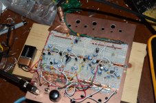
take a look at the picture.
I stilll can't agree on the PTH though, if I'm just going to solder on top then I can just use the board upside down. At that point why even have it drilled at all? Seriously though, I hear you and I think we are looking at the idea very differently. Thanks for your input.
If just for proving idea, I use the stick in wires breadboard. In fact I designed quite a few guitar pedals all on those boards. Those are for low current circuits, but for preamps, it's perfect. In fact I set it up with mux switch that I can build 4 different circuits and jump between one to the other instantaneously to compare sound. No soldering, just plug in components and wires.
I am at the process of building mix breadboard and tube socket for tube preamps. I just put all the HV components onto the pcb that hold the tube sockets and put all the tone stack and others onto the breadboard that I use plug in wires. BUT I found tube circuits are very sensitive to layout. I ended up still building into the amp chassis.
I have a lot of problems peeling traces with a non plate through holes. It serve as anchor to make the trace stronger to take a beating.
Attachments
Last edited:
why does PTH make removal harder?
A little bit, but it's all about technique. In some case, I find it harder. With PTH, I can desolder components and put in new components from the top without removing the board to get to the bottom. Most of the time, removing the board is the biggest inconvenient part. Without PTH, you can remove the component maybe twice before the trace gets ripped out.
The important thing is it's cheap to do PTH now. PTH is a two layer board, you can design traces on both side, that makes a day and night difference in layout and circuit performance. You can easily avoid ground loop, shorten the sensitive input traces etc.
I did a few runs of 2.5" X 1.25" two sided boards on ebay. 5 boards run for $50 USD. I am very happy with it, I have no plan or interest in edging boards myself. You can go on ebay and sent the Gerber file to get a bid.
Last edited:
Fairy nuff. I generally don't have a problem. Having said that, since I scored a second hand metcal cheap my soldering seems a lot more competent.
Back on topic, the main problem with the proto board I'm currently using (skip find at work years ago) is that it only has 2 power rails. Which is a pain when doing stuff that has a negative rail.
I gave this a lot of thoughts, there is no graceful way. That's the reason I just go the easiest by using wire plug in breadboard for proving. They are all bad, so might as well do it the easiest way. It works for me in many guitar pedal designs. I build those, have people comment on it, then improve before put it in real PCB.
A double sided board with no PTH and with copper tracks troughout the length at double spacing and 90 degrees to each other would be an alternative. In some zone you can keep area for ICs' prototyping.
Gajanan Phadte
Gajanan Phadte
I think this one may fullfill many requirements :
Germany
UP 941EP: Laborkarte, Epoxyd, 160x100mm, CU 35µ bei reichelt elektronik
England
Tools Equipment/PCB Equipment/PCB Prototyping/Prototyping PCBs | Rapid Online
I found this post where the author used it, the current price seems to be half that he quoted :
http://www.diyaudio.com/forums/ever...ur-vero-board-designs-here-5.html#post3662343
The thread is gorgeous, I love these achivements :
http://www.diyaudio.com/forums/ever...ur-vero-board-designs-here-3.html#post2603386
http://www.diyaudio.com/forums/ever...ur-vero-board-designs-here-6.html#post3884918
- Status
- Not open for further replies.
- Home
- Design & Build
- Parts
- Generic Prototyping Board For Audio