I've been putting off a couple of projects because I don't have a nice solution for IEC C14 power entry, voltage surge protection, inrush current limiting, and dual voltage selection (I have family in the good ol' US of A).
I recently built Pete Millett's fantastic NuClassD (write up to follow soon) and its accompanying PSU. I thought his solution was absolutely top notch. After a few nights of searching and coming up blank I decided to have a bash at a PCB design of my own. I use the term 'own' somewhat loosely as it really is heavily lifted from Pete's work.
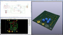
Here's what I've come up with: GitHub - baseonmars/iec-power-entry-module: A 'universal' IEC C14 power entry module with fuse, switch, MOV and inrush current limiting. - It's the first PCB I've designed, seems to pass JLC PCB's online checker.
I'm thinking 1.6mm board with 2 oz copper and immersion gold finish.
I'm not a trained EE by any stretch so I wondered if I could get a little feedback on both safety and possible features. If there's any interest I'd be happy to run a group buy as It looks like most of the cost is in processing and postage rather than number of boards.
I recently built Pete Millett's fantastic NuClassD (write up to follow soon) and its accompanying PSU. I thought his solution was absolutely top notch. After a few nights of searching and coming up blank I decided to have a bash at a PCB design of my own. I use the term 'own' somewhat loosely as it really is heavily lifted from Pete's work.
Here's what I've come up with: GitHub - baseonmars/iec-power-entry-module: A 'universal' IEC C14 power entry module with fuse, switch, MOV and inrush current limiting. - It's the first PCB I've designed, seems to pass JLC PCB's online checker.
I'm thinking 1.6mm board with 2 oz copper and immersion gold finish.
I'm not a trained EE by any stretch so I wondered if I could get a little feedback on both safety and possible features. If there's any interest I'd be happy to run a group buy as It looks like most of the cost is in processing and postage rather than number of boards.
Attachments

Last edited:
are you sure the circuit is correct ?
it looks thermistor is across primaries and not in series.
maybe i just read it wrong ?
it looks thermistor is across primaries and not in series.
maybe i just read it wrong ?
your traces look incredibly tiny. you can increase those by specifying yourself in the KiCAD settings.
A trick that I use to 'fuse' power traces in the event of a short, is to make the trace slightly smaller at the power connections themselves (a smaller width trace section in a specific place). This way if there's a short, it will break in a known spot and still allows a high current trace, since the majority is nice and wide. Not sure if I made myself clear, but...
A trick that I use to 'fuse' power traces in the event of a short, is to make the trace slightly smaller at the power connections themselves (a smaller width trace section in a specific place). This way if there's a short, it will break in a known spot and still allows a high current trace, since the majority is nice and wide. Not sure if I made myself clear, but...
In terms of trace width, the current board would be rated for just between 0.25A or 0.5A (is this an external layer in air? It'll be covered by a solder mask) - I agree that's not really very 'universal' - it's likely fine for most applications with a transformer in the UK but cutting it fine in the US. The traces are 2mm in width.
Copper thickness quoted by the fab house is 75um, I used this calculator to derive the current rating - Printed Circuit Board Trace Width Tool | Advanced Circuits
In terms of spacing I've seen figures quoted between 2.2mm and 4mm, obviously this is a case of more is better so I'll see what I can do.
Thicker traces will reduce the gap in places so I think sensible next steps is to look at hardware with a larger pitch.
Thanks for the helps so far, I'll post an updated design when I get a chance along with some calculations.
@JPs64 Can you go into more detail? If German is easier I can ask a friend to translate.
Last edited:
You‘re working with letal voltages so you‘ve to respect some rules according DIN EN 60664-1 or other standards.
My 2 cents,
JP
My 2 cents,
JP
perfect @JPS64 - that's very useful - I'll read up on it. What's the search term I should be looking for to find other related rules/specifications?
High Voltage PCB Design: Creepage and Clearance Distance | PCB Design Blog | Altium seems like a good resource - am I missing out on anything by following this advice?
It also looks like KiCad has some calculators built in that relate to the standards mentioned - https://docs.kicad-pcb.org/5.1/en/pcb_calculator/pcb_calculator.pdf
It also looks like KiCad has some calculators built in that relate to the standards mentioned - https://docs.kicad-pcb.org/5.1/en/pcb_calculator/pcb_calculator.pdf
Last edited:
Since you are fused at entry, you shouldn't have to worry as much about faults. Don't be afraid of making some robust traces.
I practice tucking planes and traces under and behind things so that they either dont have or is harder to have a chance of shorting. Your post actually made me redesign my PCB mounted entry this morning. Was goodie, but now goodier. I studied the fab house thicknesses and layers and prepreg and got OCD.
I practice tucking planes and traces under and behind things so that they either dont have or is harder to have a chance of shorting. Your post actually made me redesign my PCB mounted entry this morning. Was goodie, but now goodier. I studied the fab house thicknesses and layers and prepreg and got OCD.
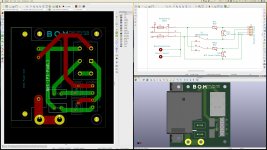
So a few changes and updates - track width enlarged slightly, minimum spacing enforced through settings and footprints updated.
I found 3D models for many parts (a mixture of Mouser and SnapEDA) which at least for me makes it a bit easier to visualise spacings. Mounting holes have been increased to allow for a little wiggle room and spacing has been adjusted to whole numbers - with any luck this will fit on a modushop mounting board.
Github has been updated with the latest files if you're interested: https://github.com:baseonmars/iec-power-entry-module.
Thank you all for your help. I've learned where to find standards/recommendations, how to source and make my own footprints and soon I'll hopefully learn the joy of holding the finished working product in my hands.
Attachments
JP - the spec I found suggest 0.4mm is the distance I need to respect. I’ve got more than that here. What kind of numbers are you suggesting?
I suggest following spacings according DIN EN 60664-1 (cat. II) and 230VAC:
- 3mm between L and N
- 6mm between L or N and Earth (pay attention to screws and washers M3 > 6mm diameter)
JP
- 3mm between L and N
- 6mm between L or N and Earth (pay attention to screws and washers M3 > 6mm diameter)
JP
Thanks JPS64! That is a very big help. The published parts of that spec that I was able to find didn't mention those numbers, even WWW.CREEPAGE.COM Welcome! comes out with figures of half those. I'll come back with a revised design soon. Really, thank you very much!
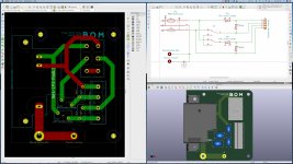
More adjustments to make allowances for creepage distances of 3mm L to N and 6mm PE and anything.
The spacing of the DD21 power pins is pretty tight but I got there in the end, 3.8mm of clearance between the tracks L and N pins. I did consider switching out for a DD22 but in the end the larger size and price was off putting.
Clearance is set to 3mm but in practice many components and tracks are further apart. I upped the pitch size on the NTCs and MOVs to allow for more spacing and the 7.5mm pitch power connector will end up being quite welcome. Ground pins have 6mm tracks and 6mm clearance.
Feedback really will be gratefully received - it's been at times frustrating (especially with KiCad ceasing up) but in the end it was quite an enjoyable exercise.
Attachments

Thank you very much @JPS64. Warnings added and uploaded to GitHub: GitHub - baseonmars/iec-power-entry-module: A 'universal' IEC C14 power entry module with fuse, switch, MOV and inrush current limiting.
- Home
- Amplifiers
- Power Supplies
- Generic Power Entry PCB