I've decided that it would be a bad idea to hijack the other thread, so i've started my own one 🙂
this is based on rod ellios design at
http://sound.westhost.com/project19.htm
this is based on rod ellios design at
http://sound.westhost.com/project19.htm
Attachments

Sorry nuuk, i wasnt expecting the post to be held in captive in customs because im a new member 😉
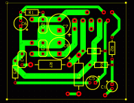
Anyway, I was wondering if there are any possible signal problems(such as interference from power rails) or if any ground loops have occoured, as for note the input(pin 10) is actually a bipolar,however expresspcb didnt have bipolar round pronged capacitors 🙂
Anyway, I was wondering if there are any possible signal problems(such as interference from power rails) or if any ground loops have occoured, as for note the input(pin 10) is actually a bipolar,however expresspcb didnt have bipolar round pronged capacitors 🙂
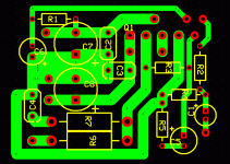
This looks professional, gj and mine looks kinda ghetto. What's the benfit of a wider piece of copper?
I'm not really familar enough with this design to comment if there are any problems or not. Which chip are you intending to use with it?
Ok, the chip i'm going to use is the lm3886, however this board is compatible with the lm3876(below pin 1 and pin 5 is a set of holes for a jumper to go into to connect both of the v+'s together(required for 3886, according to the docs)
R6 has a .7 microhenry inductor wound around it(enamaled copper winding..), however directly underneath there is a ground plane the negative signal of the opamp(including feedback) is running directly under the inductor. Are you able to see any track placement related problems that could arise if this board was etched and used?
R6 has a .7 microhenry inductor wound around it(enamaled copper winding..), however directly underneath there is a ground plane the negative signal of the opamp(including feedback) is running directly under the inductor. Are you able to see any track placement related problems that could arise if this board was etched and used?
S.C said:This looks professional, gj and mine looks kinda ghetto. What's the benfit of a wider piece of copper?
larger track width is required as the current going through the tracks increases, eg. if you were to use 1mm tracks with currents of 80amps going through it.. you would turn the track into a resistor, it will burn continue burning until something breaks the link(eg boom or crack!) 🙂
Hi,
my suggestion:
- delete track between R4 and R5
- place R6 parallel to R7 (speaker output move to left side of PCB)
- move R5 close to C5
- place track (30mils) between signal ground (pin7, R4,R5, shield of input signal cable ) and power ground (C4,C6,C2,C3)
Regards
my suggestion:
- delete track between R4 and R5
- place R6 parallel to R7 (speaker output move to left side of PCB)
- move R5 close to C5
- place track (30mils) between signal ground (pin7, R4,R5, shield of input signal cable ) and power ground (C4,C6,C2,C3)
Regards

- Status
- Not open for further replies.
- Home
- Amplifiers
- Chip Amps
- Gainclone layout check..