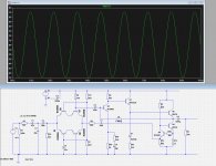
I was idle so decided to find out what this simulator does - came up with an exercise in gain/bandwidth - thought I'd ponse around with a few circuit ideas.... I initially had a line input stage in mind at first.
I thought I'd go whacky and wierd and use something often done in RF amps -- use the emitter as the inlet ....what fun .... now I'm having coffee and cake.
Does anyone know how accurate these stimulators ....*cough*...I mean simulators are.... I'm not experienced in using them
I thought I'd go whacky and wierd and use something often done in RF amps -- use the emitter as the inlet ....what fun .... now I'm having coffee and cake.
Does anyone know how accurate these stimulators ....*cough*...I mean simulators are.... I'm not experienced in using them
Attachments
Sometimes its error cannot be tolerate😕, btw what is this opamp used for? its looks like strange.
Hi
As I said I was just mucking about with a semi daft idea of having a common base input for a line board.
Common base mode is not generally used in audio. Common base mode tends to feature in FM radio designs as the input from the antenna - the bandwidth is extreme and input impedance is very high, before FETs were commercially available. If one were to remove the front end... remove C7 drop the value of C9 and reconfigure the input values for maximium gain - this will operate well into the RF
I wonder how close the simulator matches real life - will it calculate the BJT load capacitance CBc and BEc?
I ever use simulator to simulating some type of FM oscillators and resulting only small differences from the real circuit, but when I placing buffer and two more stage of amplifier on it, it become totally different from the real.
small error + small error + small error x small error / small error = total error. This is what simulator do.
Yes it has. Using different type of transistor or changing its model will produce different result.
Using BF959 and 2N2222A for 100mhz simulation will be big differences.
small error + small error + small error x small error / small error = total error. This is what simulator do.
Yes it has. Using different type of transistor or changing its model will produce different result.
Using BF959 and 2N2222A for 100mhz simulation will be big differences.
Last edited:
Have you measured the input impedance 😉
Collector of Q7/8 ?
That would make the input impedance zero, Mooly -- it's not zero
or were you joking?😉
 Ha ha ... otherwise you wouldnt get 40x gain
The point I'm actually trying to grasp -- is how good are these simulators?
Last edited:
Just build it and see what happens.
Q7/8... Collectors have no DC path anywhere.
Q6... looks like you are attempting a constant current source... look at the value of R12.
You will only know how good the simulator is by building and measuring for real... so try it 🙂
Q7/8... Collectors have no DC path anywhere.
Q6... looks like you are attempting a constant current source... look at the value of R12.
You will only know how good the simulator is by building and measuring for real... so try it 🙂
Ahhhh I see what you're getting at 😉
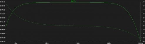
Yup - it's not a CCS - its only a neg feedback inject, playing with gain/bandwidth product - infact if I put a path right there to DC, according to simulator gain reduces and bandwidth reduces because then it is decreasing input impedance.
If I remove that feedback path entirely - the gain remains the same - but bandwith goes beyond what I think the BD139s are capable of - it potentially shoots off to 30 Mhz. Be great as a first stage of a radio. Which is where I was wondering if this simulator thing is picking up the Base emitter and collector base capacitive properties in the junctions? I'm suspecting not.
I love experimentation and I am building it to find out
Last edited:
- Status
- Not open for further replies.
- Home
- Amplifiers
- Solid State
- Gain/bandwidth - pre amp