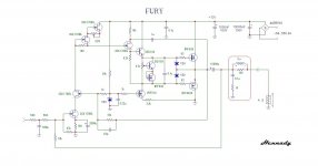
I decided to highlight this scheme as a separate topic, because a concept has been formed both in terms of topology, element base, correction features, and, in fact, sound.
This scheme was called Fury (FURY).
circuit features:
1) the circuit of the voltage amplifier on JFET transistors in cascode inclusion
2) two NFB circuits, one of which covers the output capacitor, the second also corrects the stability (taken from the output of the amplifier)
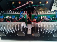
3) complementary hexfet output
4) deep NFB (not less than 70dB)
5) inverting inclusion
The block diagram of Fury consists of three stages:
1st cascade on the field (jfet) with inverting inclusion
2-nd cascade of field devices (jfet) with dynamic load and low-impedance output for coordination with output stage
3rd cascade single follower with high-resistance input and with dynamic load + push-pull output stage on hexfettes in class AB
The nuances of the scheme:
* the first two stages without load have a gain of 95dB
* The contour of NFB at the input determines the overall gain of the circuit at 19.2 dB
* maximum input voltage (amplitude 3 volts)
* added RC input f = 816kHz to reduce dynamic distortion
* the second NFB circuit goes to the gate of the second stage, it is connected relative to the reference voltage of 13 volts (implemented on the zener diode), this circuit carries out correction of the amplifier at high frequencies for its stability and sets the operation mode of the output stage by constant voltage.
P.S. In the event of a break in any of the negative feedback loops or two at the same time, the circuit remains operational.
Nuances of the scheme of the 3rd cascade:
* at the input a field + bipolar transistor, which takes a signal from the source of a stable current source, because lower pre-amplifier output impedance is needed to match these stages
* dynamic load performed on mosfet IRF510
* The bias circuit of the output stage is made on the BD139 transistor with the IRF530 transistor - it provides smooth adjustment of the initial current of the output stage 100mA
* The thermosensitive element is the BD139 transistor, it is he who is screwed to the radiator.
* The use of IRF630 / 9630 turned out to be quite a musical complementary pair ...
Circuit Parameters:
* Ku = 19.2dB
* Uin max ~ 3V (amplitude), Uin nom ~ 2V (amplitude)
* P out (RMS) max = 40 watts (4 Ohms)
* slew rate SR = 5.84V / microS
* Frequency response in the frequency range 1-100000Hz is 0.05dB
* uneven phase response -1.5 degrees (20 kHz) and -7 degrees (100 kHz)
* delay at a frequency of 100 Hz - 0.24 microS, at a frequency of 20 Hz - 1.4 microS, at a frequency of 5 Hz - 96 microS
* output impedance R (i) 0.34 ohm ...
* the depth of the negative feedback in the frequency range 1-1000Hz is 76dB, at a frequency of 20kHz - 70dB
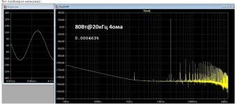
* THD distortion (nominal) at a frequency of 1 kHz less than 0.001% (0.0004%), at a frequency of 20 kHz - 0.006%
* initial current of the output stage 100mA
* power scheme - you can use unstabilized
This scheme was called Fury (FURY).
circuit features:
1) the circuit of the voltage amplifier on JFET transistors in cascode inclusion
2) two NFB circuits, one of which covers the output capacitor, the second also corrects the stability (taken from the output of the amplifier)
3) complementary hexfet output
4) deep NFB (not less than 70dB)
5) inverting inclusion
The block diagram of Fury consists of three stages:
1st cascade on the field (jfet) with inverting inclusion
2-nd cascade of field devices (jfet) with dynamic load and low-impedance output for coordination with output stage
3rd cascade single follower with high-resistance input and with dynamic load + push-pull output stage on hexfettes in class AB
The nuances of the scheme:
* the first two stages without load have a gain of 95dB
* The contour of NFB at the input determines the overall gain of the circuit at 19.2 dB
* maximum input voltage (amplitude 3 volts)
* added RC input f = 816kHz to reduce dynamic distortion
* the second NFB circuit goes to the gate of the second stage, it is connected relative to the reference voltage of 13 volts (implemented on the zener diode), this circuit carries out correction of the amplifier at high frequencies for its stability and sets the operation mode of the output stage by constant voltage.
P.S. In the event of a break in any of the negative feedback loops or two at the same time, the circuit remains operational.
Nuances of the scheme of the 3rd cascade:
* at the input a field + bipolar transistor, which takes a signal from the source of a stable current source, because lower pre-amplifier output impedance is needed to match these stages
* dynamic load performed on mosfet IRF510
* The bias circuit of the output stage is made on the BD139 transistor with the IRF530 transistor - it provides smooth adjustment of the initial current of the output stage 100mA
* The thermosensitive element is the BD139 transistor, it is he who is screwed to the radiator.
* The use of IRF630 / 9630 turned out to be quite a musical complementary pair ...
Circuit Parameters:
* Ku = 19.2dB
* Uin max ~ 3V (amplitude), Uin nom ~ 2V (amplitude)
* P out (RMS) max = 40 watts (4 Ohms)
* slew rate SR = 5.84V / microS
* Frequency response in the frequency range 1-100000Hz is 0.05dB
* uneven phase response -1.5 degrees (20 kHz) and -7 degrees (100 kHz)
* delay at a frequency of 100 Hz - 0.24 microS, at a frequency of 20 Hz - 1.4 microS, at a frequency of 5 Hz - 96 microS
* output impedance R (i) 0.34 ohm ...
* the depth of the negative feedback in the frequency range 1-1000Hz is 76dB, at a frequency of 20kHz - 70dB
* THD distortion (nominal) at a frequency of 1 kHz less than 0.001% (0.0004%), at a frequency of 20 kHz - 0.006%
* initial current of the output stage 100mA
* power scheme - you can use unstabilized
Attachments
Last edited:
The bias pot is in an amp-self-destruct configuration. You should arrange than if the wiper loses connection with the track that the bias voltage drops, not rises, since this can happen with dirt on the track and you don't want to burn out the output stage if this happens. You'd normally have fixed resistor base-collector, pot on base-emitter, pot fails, the transistor conducts hard, bias drops, amp is safe.
While talking about the bias arrangement - why have that FET on the Vbe emitter?
Why are the protection zener's connected like that - it looks like they could easily become forward biased in the opposite half cycle. Normally back-to-back zeners or TVS diodes would provide protection without limiting gate-source voltage polarity.
You have chosen non degenerated outputs, I firmly in accordance with you . But, the bias to follow thermally is wrong, the thermal drift of MOSFETs at 100ma is about -4mv/C°. I glue with silicon a paire of 1n4148 in series upon each output. By this your bias circuit becomes four diodes and a resistor in series.
I wonder how much is the drop out of this circuit ?
I wonder how much is the drop out of this circuit ?
Last edited:
thanks, but this is a matter of practical implementation of the scheme.The bias pot is in an amp-self-destruct configuration. You should arrange than if the wiper loses connection with the track that the bias voltage drops, not rises, since this can happen with dirt on the track and you don't want to burn out the output stage if this happens. You'd normally have fixed resistor base-collector, pot on base-emitter, pot fails, the transistor conducts hard, bias drops, amp is safe.
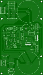
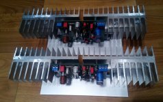
Now in the working stereo layout, as in the diagram in the attachment.
they exclude temperature overcompensation of the output stage, while the bias has a low differential resistance....While talking about the bias arrangement - why have that FET on the Vbe emitter?
these are protective diodes, are more needed when the amplifier is turned on, because DC output voltage rises very slowly when the amplifier is connected to the network. In other modes, these zener are turned off....
Why are the protection zener's connected like that - it looks like they could easily become forward biased in the opposite half cycle. Normally back-to-back zeners or TVS diodes would provide protection without limiting gate-source voltage polarity.
One can clamp the bias pot with 2 or 3 1n4148 to limit bias if the pot wiper lets go.The bias pot is in an amp-self-destruct configuration.
I like the single supply, I have transformers of that voltage. I like speaker caps if a solder joint lets go & Dc occurs. My speakers cost 6 times what an amp does, 20 * on surplus transformers & case.
I like you used available vfets. The 2sk170 is a unicorn, not available in the US from newark,digikey,mouser,arrow. How does it perform on J111 J112 or J113 which can be bought without involving a counterfeit house or customs thieves? Or some other On semi or ST part. Don't tell me about surface mount parts. SM adapters are $8 each if I don't send my debit card # to the orient for hacking.
If the wiper pot lets go a clamp can only restrict you to the maximum of the adjustment range, which is going to be pretty high in a practical circuit which has to cope with component tolerances, so that the adjustment end ranges are quite wide of the operating area.
The rise in bias current with bias voltage is exponential so its really easy to fry things this way.
The rise in bias current with bias voltage is exponential so its really easy to fry things this way.
these are protective diodes, are more needed when the amplifier is turned on, because DC output voltage rises very slowly when the amplifier is connected to the network. In other modes, these zener are turned off.
No, they switch on (forwards mode) when the opposite output device is driven hard. Unless the voltage across the gate-source is less than 0.6V, which it won't be AFAICT. But then again I've not checked the typical curve for that MOSFET, so maybe you get away with this, but in general you can't.
Last edited:
yes, only these are transistors with an index BL, i.e. 2sk170BL...
I like you used available vfets. The 2sk170 is a unicorn, not available in the US from newark,digikey,mouser,arrow. How does it perform on J111 J112 or J113 which can be bought without involving a counterfeit house or customs thieves? Or some other On semi or ST part. Don't tell me about surface mount parts. SM adapters are $8 each if I don't send my debit card # to the orient for hacking.
if you use J111-113, it will work, only it will be necessary to increase the resistor at the source of the voltage amplifier and the current source to 510 ohms. The distortions will increase alas by 20 times ...🙁
It is interesting, to try j114, the distortions are small no more than 0.008%, but this is still more than with 2sk170BL...
ok i don't mind using bidirectional zener.No, they switch on (forwards mode) when the opposite output device is driven hard. Unless the voltage across the gate-source is less than 0.6V, which it won't be AFAICT. But then again I've not checked the typical curve for that MOSFET, so maybe you get away with this, but in general you can't.
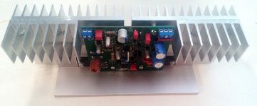
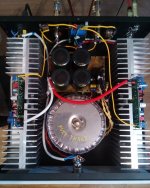
The working scheme, there are no problems yet, it turns on silently - all operating points are in modes ...
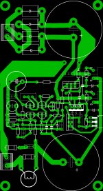
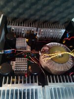
Now he is busy combining boards with a power supply, so this board turns out ...
Attachments
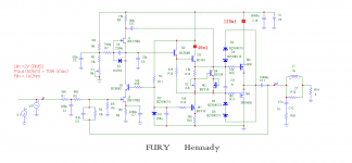
Hello!
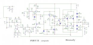
the scheme that went into practical implementation, see attachment.
the circuit has a relatively low input impedance, but it is enough to work with modern devices, for example, output from Laptop cards or DAC with a buffer ....
The circuit has 1 gain stage 84dB Open Loop with a pole at a frequency of 7kHz and a unity gain frequency of 5MHz.
Distortion is less than 0.001% at all frequencies up to 50 watts of output power, at maximum power it increases to 0.005% at a frequency of 20 kHz ...
Attachments

Last edited:

Yes, initially its task was to increase the input impedance at high frequencies for Q1 in order to increase the linearity of the input JFet (J2), in practice this internal NFB conflicted with the correction circuit at the input due to the spread of the parameters of its elements, and it also reduced the Slew Rate due to the fact that it took part of the output current from transistor Q3.
The next stage in the evolution of the circuit is a composite version of the circuit using an operational amplifier.
It became possible to use a volume control at the input and, due to the use of a 250VA transformer, to apply parallel connection of output mosfets.
circuit features:
1. at the input volume control X1 with a nominal value of 50 kOhm (ALPS), the engine is shunted with resistors R1R2 with such values at which, in any position of the volume control, its actual value was not more than the value of the resistor R3 at the input of the microcircuit Х2 (OPA2134). This results in minimal influence of the volume control on the transient response of the amplifier.
2.Also removed the capacitor from the source of J2, this increases the linearity of the circuit and the sound is less dependent on the components of the circuit.
3. when output mosfets are connected in parallel, it is not necessary to use equalizing resistors in the sources. In my case, when connected in parallel, the maximum power increased to only 90 watts into a 4 ohm load, but the damping of the speaker system was improved.
4. For stable operation of the op-amp at the input with a composite solution, because the negative feedback input falls on the non-inverting input of the X2 microcircuit, I used the T-shaped NFB R6R7R9, the advantages of such a solution in the use of low-resistance resistors in the NFB circuit, tk. at the non-inverting input, the frequency properties are worse.
Thus, the gain of all circuits is obtained as follows: Ku= 1 + (R6 + R7 + (R6 + R7) / R9) / P4 = 1 + (2k + 2k + (4k/1k)) / 1 = 9 (or 19.1 dB)
although as a result of the composite solution, the slew rate was reduced, the distortions were reduced by 2 times and at a frequency of 1 kHz with an output power of 50 watts amounted to 0.0002%.
in general, it was this decision that was chosen as positive during test auditions.
Attachments
I wasted a download on Fury II because single supply, before I spotted the LSK170 . Diyaudio did a group buy of these about 5 years ago, and there has been nothing but fakes available since. Like lateral fets, great parts, never available, and the 2nd source of those has shut down.
I'm confused. I see around 6000 available on digikey. Has LSI shut down?I wasted a download on Fury II because single supply, before I spotted the LSK170 . Diyaudio did a group buy of these about 5 years ago, and there has been nothing but fakes available since. Like lateral fets, great parts, never available, and the 2nd source of those has shut down.
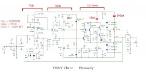
The next step was the Fury three scheme, which differed in that it was essentially a composite version on discrete elements.
The input stage from Furia was used as an input voltage amplifier with a gain of 77 dB without negative feedback, a second stage was added with a gain of 36 dB with a level shift relative to ground.
The follower for the output transistors has become a structural assembly for maximum linearity and maximum +/-32 swing without being limited by a +/-36 volt bipolar supply.
Output transistors - MOSFETs IRFP 240/9240
The scheme also uses progressive correction. Distortion at a frequency of 50 watts (4 ohms) at a frequency of 1 kHz is 0.000012%
Amplifier module in attachment
Attachments
- Home
- Amplifiers
- Solid State
- FURY amplifier