Hi guys,
I have for sale vector network analyzer - VNA N2PK:
( www.makarov.ca - N2PK VNA Project )
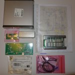
- completely assembled PCB for 1x N2PK VNA and 1x reflection bridge
- metal Hammond case for VNA and RFbridge
- completely assembled PCB for PSU ver. 3 kit (latest version) by OM3LZ specially designed for VNA (5, 9 and 12v)
ship to: EU
price: 500 EURO ( ex-work incl. shipping and paypal fees )
payment options: paypal
contact: milandks at pobox.sk / Slovakia
regards
milandks
I have for sale vector network analyzer - VNA N2PK:
( www.makarov.ca - N2PK VNA Project )
- completely assembled PCB for 1x N2PK VNA and 1x reflection bridge
- metal Hammond case for VNA and RFbridge
- completely assembled PCB for PSU ver. 3 kit (latest version) by OM3LZ specially designed for VNA (5, 9 and 12v)
ship to: EU
price: 500 EURO ( ex-work incl. shipping and paypal fees )
payment options: paypal
contact: milandks at pobox.sk / Slovakia
regards
milandks
Attachments
Last edited:
milandks,
Most people here would be interested in things like frequency/phase response over the extended audio bandwidth, say 10Hz to a few MHz. And impedance measurements, same frequency range.
Can we do that with this unit? Can you show some examples?
Jan
Most people here would be interested in things like frequency/phase response over the extended audio bandwidth, say 10Hz to a few MHz. And impedance measurements, same frequency range.
Can we do that with this unit? Can you show some examples?
Jan
Hello Jan,
The basic frequency range VNA is from 0.05 to 60MHz, but works sort-of-ok down to 15 KHz or so. That establishes a baseline inside the audio range where the response is flat.
More info's about the possibilities of measurement you can find here:
N2PK Amateur Radio Projects Page - Paul Kiciak
myVNA
I had a plan to detect optimal compensation for small audio PA system via open-loop phase margin. For more info's You can see this article: Ochoa, A. Jr., "Finding phase margin of feedback systems from closed loop AC simulations," Circuits and Systems, 2000. Proceedings of the 43rd IEEE Midwest Symposium on, Vol. 3, p. 1228 - 1231.
Inspiration and other details gave me Gary Johnson, he's RF engineer.
Today, I do not have any particular measurement.
Regards
Milan
Hello Jan,
The basic frequency range VNA is from 0.05 to 60MHz, but works sort-of-ok down to 15 KHz or so. That establishes a baseline inside the audio range where the response is flat.
More info's about the possibilities of measurement you can find here:
N2PK Amateur Radio Projects Page - Paul Kiciak
myVNA
I had a plan to detect optimal compensation for small audio PA system via open-loop phase margin. For more info's You can see this article: Ochoa, A. Jr., "Finding phase margin of feedback systems from closed loop AC simulations," Circuits and Systems, 2000. Proceedings of the 43rd IEEE Midwest Symposium on, Vol. 3, p. 1228 - 1231.
Inspiration and other details gave me Gary Johnson, he's RF engineer.
Today, I do not have any particular measurement.
Regards
Milan
Hello Milan,
Eevn if I am not getting your VNA, would it be possible for you to send me a PDF of this article you quoted? I would be very grateful. jandidden01 at gmail dot com
As a return, maybe this is useful for you:
https://www.researchgate.net/public..._Determination_in_a_Closed-Loop_Configuration
Thanks,
Jan
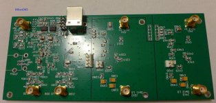
Are you sure these boards where tested and they work? Nothing worse then someones project that is fine, but when you get it then the problems start, and this not being a big production item... your hosed and lose every and parts bring $.25 for all of them.
Cap C177 and C170 look damaged by solder. A process indicator for sure.
Some look to have too much solder drooping down in the pads while others part have it over into the body of the part....not a good sign.
Then on the second board, L172 broken ? L180 looks to have is end burned off. Similar soldering done there also.
C185a missing most of the end and solder on the side?
What happened with U110 on the second board? Looks like a mess there on the pins across from pin1.
Then there is C480, C5481, C482...some look burned, others look like missing some solder.
Above that C450 looks like a side is missing solder.
Soldering on the right side of the boards looks better than the left side.
Were they learning SMT as they were going along and figured it out
on the right side of the board?
SCARY to buy this....
Are there any step by step assembly instructions?
Or just the schematic?
Cheers,
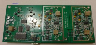
Last edited:
Thank you, this was your most funny comment.
All boards have been assembled and soldered in a professional company that has many years of experience with electronic parts and HF transmitters.
And yes, all boards have been tested and are ok.
Are you expert on quality of the PCB from the pictures?
Have you any certificates?
regards
milandks
All boards have been assembled and soldered in a professional company that has many years of experience with electronic parts and HF transmitters.
And yes, all boards have been tested and are ok.
Are you expert on quality of the PCB from the pictures?
Have you any certificates?
regards
milandks
It wasn't meant to be funny, as I'm interested in thisThank you, this was your most funny comment.
unit, I think anyone would ask the same thing.
I didn't see anything that mentioned the company of manufactureAll boards have been assembled and soldered in a professional company that has many years of experience with electronic parts and HF transmitters.
And yes, all boards have been tested and are ok.
nor acceptance nor proof that they actually work and perform as intended.
Are you expert on quality of the PCB from the pictures?
Have you any certificates?
I've described the issues that I saw quickly.
and they conform to IPC-A-610, Acceptability of Electronic Assemblies.
For example, Chapter 12, (various paragraphs)
Surface Mount Assemblies:
Defect - Class 1,2,3
Solder fillet extends onto the component body.
Defect - Class 1, 2
A properly wetted fillet is not evident.
Defect Class 3
Minimum fillet hight (F) is lass than solder thickness (G)
plus 25% (H). Or, solder thiickness (G) plus 0.5mm [0.02in],
whichever is less.
Defect - Class 1,2,3
Insufficient solder.
Defect - Class 1,2,3
Less than minimum acceptable end joint width.
(End joint widch (C0 is minimun 50% of component
termination width (W) or 50% land width (P), whichever is less.)
Anyone looking at the pictures you've posted
and reading these defect classes, it should be self evident.
Cheers,
Last edited: