Hi,
where did this schematic come from?
Why 1n4007 diodes when the worst case reverse voltage must be <=1V?
300uA passing each of the LTP inputs seems a bit low.
Are the VAS transistors upside down?
Are the 340/350 suitable for VAS duty?
Why 10r for the lower driver emitter?
MJE15030/31 is the type code.
Change the bias pot so that failure/intermittent wiper does not over bias the output stage.
Add Zener protection to the output Gates.
Why do the monitoring side of the CCSs require ~8mA and the VAS only 2mA?
Where are the output source resistors?
Who is still claiming 1200W into 4r0? This needs 98Vpk and 24.5Apk into a resistive load. Where does this ability come from? and somewhere around 70Apk into a reactive speaker load!
Someone did not think about this.
There is a thread running here, as I stated before, regarding THIS schematic.
Anthony Holton is quite 'mad' because of that.
This is the origin of all this thread: http://www.lateralmosfet.com/Lateral Mosfet Datasheet.pdf
Same schematic...
I don't know if it is exactly the one Anthony Holton uses.
If it is, it must work, with LFets... Not VFets...
Sure, netuddki is playing around with some 'addons' to the original schematic.
For sure, with those IRFP90N20/P20 this will not work...
Neither will give 1200W...
BTW, why that 'bias' transistor?
black said:netuddki posting your pcb in sprint layout
Attachments
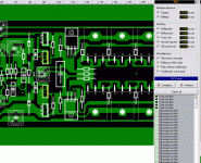
audioDIYer said:A little messy...
Quite a lot of errors with DRC...
BUT WORKING!!!
")
netuddki said:
BUT WORKING!!!
Have you etched the pcb?
Have you soldered all components?
Have you powered it up?
Have you done something but working with sPrint Layout?
I'm asking because I'm interested on results.
To Andrew T:
Blue or grey smoke?... Let's bet
audioDIYer said:
Have you etched the pcb?
Have you soldered all components?
Have you powered it up?
Have you done something but working with sPrint Layout?
I'm asking because I'm interested on results.
To Andrew T:
Blue or grey smoke?... Let's bet
I will!!
I will send you a pictures!

25A peak into a 4r0 resistive load.
It could approach 70Apk on fast transients into a reactive load if it were capable of 1200W into 4ohms
It could approach 70Apk on fast transients into a reactive load if it were capable of 1200W into 4ohms
Who is still claiming 1200W into 4r0? This needs 98Vpk and 24.5Apk into a resistive load. Where does this ability come from? and somewhere around 70Apk into a reactive speaker load!
- Status
- This old topic is closed. If you want to reopen this topic, contact a moderator using the "Report Post" button.
- Home
- Amplifiers
- Solid State
- from the net