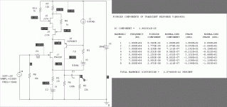
I've been messing around for about three years with various jfet/mosfet single ended preamp circuits meant to run off a 30V rail. I have a standard living room setup that allows RIAA and line amp modules to be swapped around so I can evaluate the sound. This one is a circuit using the humble and inexpensive PN4391, originally intended as a chopper/analog switch. It works very well as a cascode jfet for fancier fets like the 2SK170 and the like. It also makes a reasonable amp on its own if you can give it enough bias current to wake it up. Attached is a folded cascode circuit that provides enough current through the PN4391, and separates the load resistor from the main jfet bias so that you can tailor the gain to a desired level. I chose a gain of 40X, which is what I usually use in the the first stage of a passive RIAA preamp. I also set up the jfet and cascode transistor to be biased by strings of first-generation GaAsP LEDs, which have a low incremental resistance (I've tested it) and presumably, low noise. Each diode drops ~1.6V, and has an incremental resistance of about 1.3 ohms. The source of the PN4391 gets a string of two LEDs (3.2V, 2.6 ohms), and the cascode transistor is biased with a string of 6 (9.6V, 7.8 ohms). I expected the distortion level to be only moderately good, as the LEDs don't provide a lot of degeneration in the source of the PN4391. I tried biasing the drain of the 4391 with several current sources, starting with the perfect current source available in PSpice, and then several more practical implementations. The choice of current source affects the higher order harmonics, and the ratio of 2nd order to #rd order harmonics. The cascoded current source using a pair of J174 p-channel jfets shown in the attached schematic was one of the better performers, with almost all 2nd order harmonics. All the current sources I tried clocked in at around 0.02% THD, but with varying levels of 3rd and higher order harmonics. Next up will be a variant with a source resistor for the PN4391 instead of LED bias. I expect that the degeneration will give me lower THD, at the cost of somewhat higher noise. This may not be a really big issue at MM cartridge signal levels. The 22k output load represents the impedance of the passive RIAA network I currently like to use.
Attachments
Another variant, simpler and with lower THD, with just a resistor feeding the 4391 drain. This has been done before, but not necessarily with this fet. I'm sure the key to good performance is moving up the voltage source feeding the cascode so that it clamps the 4391 drain resistor. I'll try the same approach with a current source feed to see if the results are comparable or better. I'm applying the results of this simulation to the drive board for my "Lil Devil" hybrid tube amp - lots of parts got taken out.
Attachments

Clamping a current source with the leds did not give as good results as a simple resistor, so I won't bother showing the circuit. I was intrigued enough by the second circuit shown here to incorporate it in one of my older layouts that also uses the PN4391 in the 2nd RIAA stage. I'll post more information when I actually start to build the thing. Lots of baleful deep red LED action, both in the first stage and as a reference for the onboard shunt regulator. BTW, Electronic Goldmine has NOS National PN4391s for a quarter apiece - while they last.
Thanks for reporting these results (and to jcarr for noticing them).
Mouser shows some stock for the Fairchild PN4391, but also that it is on end-of-life status (probably the SM versions will persist, although I didn't check). A shame, as the TO92 is easier to heatsink. Better still, if one has a nice isolated dissipator, is the ancient metal can part, as the gate is common to the case.
Any reason why you used P-channel parts for your current source in the first example? As the whole shooting match floats, N-channel arrangements should work as well or better, depending upon the choice of JFET.
Brad
The p-channel option was the one that worked best - I tried several ways of skinning the cat.
I didn't try it in the simulations, but if you use more LEDs in the top bias string, you can bring down the dissipation in the jfet. There's no reason you really need 19V across the 4391. As for heat sinking, I'd just glue a little metal tab to the package with Arctic Silver epoxy. Having said that, considering the high junction to ambient thermal resistance, JB Weld might work almost as well.
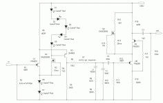
Attached is the circuit I'm considering - the whole shebang, input 40X amp, passive RIAA network, and a 30X stage afterwards.
As for the subject of availability - place your lifetime buys - jfets appear to be an endangered species. The nice thing about the 4391-4393 series is that they cost beer change.
I didn't try it in the simulations, but if you use more LEDs in the top bias string, you can bring down the dissipation in the jfet. There's no reason you really need 19V across the 4391. As for heat sinking, I'd just glue a little metal tab to the package with Arctic Silver epoxy. Having said that, considering the high junction to ambient thermal resistance, JB Weld might work almost as well.
Attached is the circuit I'm considering - the whole shebang, input 40X amp, passive RIAA network, and a 30X stage afterwards.
As for the subject of availability - place your lifetime buys - jfets appear to be an endangered species. The nice thing about the 4391-4393 series is that they cost beer change.
Attachments
Yes JFETs are, sadly, vanishing, absent some speciality houses like Linear Integrated Systems and Interfet (and they charge quite a good deal more than beer change, unless you're ordering your beer at Spago or Daniel). The SMDs will likely be around for a while though, difficult though they are to use casually.
About heatsinking: although the TO92 has a free-air dissipation rating higher than the MMBT4391 on the specified board area pattern, since the chip sits on the gate lead, that's the place to draw off the heat (NXP goes to some lengths to describe this for their BF862). When the part is used common-gate that's easier to do without incurring extra capacitance and potential interference pickup, but it's still possible with common-source or common-drain.
As to what drain-gate voltage the 4391 needs: depends on the pinchoff voltage, i.e. about the same magnitude as the "off" Vgs. For the really high pinchoff parts, they will still work but their output conductance will climb, which may spoil things in certain apps. In the PNP folded-cascode this will be less of an issue.
I do agree that the 4391 is a nice part to be a common-gate stage or driven cascade part for low-pinchoff JFETs like SK170/BF862. Porting those, with additional voltage, into some minimalist designs as replacements for single FETs can help performance markedly. And the dissipation of the "lower" device is naturally reduced, which is usually where the impact of increased drain-gate leakage becomes pertinent.
The BF862 is also cheap. I paid 22 cents a piece for 100 of them a while ago, and I just got my test socket to facilitate matching (which cost more than all the FETs!).
I'm going to go ahead and try to heat sink some parts through the case and see what the thermal imager at work has to say - we're talking about ~300mW. I dislike trying to hang stuff off the leads. I normally like to keep naked TO-92s below 100-150mW. I'll also have a look at the optimum voltage for the top LED string - I still think it can be increased some.This might also help the overall performance.
To expand on the results for alternate current sources in the first circuit, they all had similar THD in simulation, but the P-channel current source had a better mix of even harmonics vs 3rd and higher order odds. This is simulation, mind you. The simple clamped resistive load looked so attractive that I ditched the more complex scheme.
As far as that's concerned, try to find new J174/175s these days...
I also have a little roll of BF862's and a circuit waiting for them, unpublished as of yet - it's a feedback pair of the 862 and a p-channel small signal mosfet.
I have the fixture as well (a cheap clamshell socket from China), but I haven't been sufficiently motivated to put everything together and start selecting parts.
I'd only recommend the gate lead heatsinking approach for the SMD, where the lead is so close to the chip. The TO-92 at ~100mW should be fine free-air, although for thermal coupling among devices (not germane in your app) there are EUVL's TO-92 double heatsinks, more for coupling than for cooling.
People have mentioned concerns about increased thermal noise with elevated FET temps, but since we are talking about square root of absolute temperature dependence, it is usually a relatively minor consideration. In very high impedance circuits the rough doubling of gate leakage per delta 10 degrees Kelvin can quickly get ugly.
People have mentioned concerns about increased thermal noise with elevated FET temps, but since we are talking about square root of absolute temperature dependence, it is usually a relatively minor consideration. In very high impedance circuits the rough doubling of gate leakage per delta 10 degrees Kelvin can quickly get ugly.
The nasty increase in leakage with drain voltage can also be a concern, hence the attraction of a cascode. 2SK170s are very susceptible, the PN4391 series less so.
IME, although the capacitances of N-JFETs will decrease with increased drain-gate voltages, thereby speeding up the circuit, the gate leakage currents tend to ramp up rapidly with drain-gate voltage. Individual NJFETs can be more resistant to this effect, but in production quantities, I would be wary of bringing the drain-gate voltage up above perhaps 16V.
In the worst case, you may no longer be able to DC-couple a DC circuit (not applicable in this case), and noise may increase due to excess input bias currents. Both issues may force you to reduce the value of the input resistor (R6).
Again IME, P-JFETs exhibit less dramatic increases in gate leakages voltages with drain-gate voltages, so an inverted version of "PN4393-2" (P-ch input, N-ch folded cascode) may be worth trying.
What has particularly interested me about your thread is the differences in performance that you may have noted between the folded-cascode bias arrangement in "PN4393-1" (signal-driven folded-cascode) vs. "PN4393-2" and "gaincell" (constant-voltage folded cascodes).
Any insights that you can offer would be very much appreciated.
regards, jonathan carr
One observation: the first schematic may be slightly misleading, as topologically it's a driven/bootstrapped cascode, but the impedance in the source of the 4391 is very low, representing the LEDs used primarily for bias. Thus the base current from the PNP really doesn't have much effect, as it splits between the 4391 source (looking like about 1/gm under these conditions, maybe of order 100 ohms) and the LED incremental resistance, 2.6 ohms --- that is, the lion's share flows in the LEDs.
With a lot more external source resistance you will start to see the bootstrapping effect and reduction of the common-base stage distortion, and as well reduced input capacitance due to the drain-gate feedback capacitance, which is now no less than the device Cgd. Of course this will be at the expense of drastically reduced gain overall, as well as an increase in equivalent input noise voltage due to the R2 contribution.
Brad
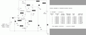
For grins, here's a cascode done standard style with a some extra current for the bottom 4391. The source is biased by a pair of GaAsP red leds, with an extra 24.9 ohms slipped in for degeneration. The gain is right where it needs to be at 40X, and the distortion is not too shabby. I like the power dissipation in all the active elements a whole lot better. This is more complex than a single cascoded 2SK170 with degeneration, with similar distortion, but the whole point was to make do with something besides that jfet for a change.
Attachments
By the way, having been away from this for some years, and prompted by your remarks and use in these circuits, I decided to look for some thread on LED noise and found this: http://www.diyaudio.com/forums/parts/35821-some-noise-measurements-leds-zener-diodes-13.html Although not the last word on the subject it has some very interesting comparative data on LEDs and zeners, and many remarks from others after the author's initial presentation and updates. And it more-or-less confirms my experience with red LEDs over the years as being decent, if not particularly low impedance, components for bias use. There are some characteristics not discussed (unless I missed it) like the temperature coefficient of the forward voltage, which makes at least standard red (GaAsP) diodes a good match to silicon base-emitter tempcos, and owing to the net voltage difference a decent component to use in simple current sources.
Brad
Brad
I have a pipeline to some of the earlier GaAsP leds from Litronix. I characterized them for use in a active cathode bias supply for a P-P tube amp. They have a lower incremental impedance than any other commonly available LED I've encountered (~1.4 ohms). I don't think anyone bothers to make this type any more, as they are not particularly efficient - you need to seek out NOS sources (possible manufacturers of similar units are HP, Monsanto, Opcoa - others might come to mind). By contrast, the common yellow-green GaP leds are about 13-15 ohms. I've tested several varieties, including HP, Liteon, and R.G. Allen (most likely some Japanese manufacturer, as R.G. Allen made a practice of re-branding Japanese parts). Noise - haven't tested that yet, but I wouldn't be surprised if the old GaAsP diodes were quiet.
I don't want to get too far off topic and be accused of hijacking your thread, but I can't resist an anecdote. When I had not been long at Harman, circa 1990, we were doing amplifiers for Ford and the sales guy came back from a trip to tell us that Ford was going to require that the trigger voltage to turn amps on would henceforth be a logic level signal. I was asked how much it would cost to make the change, and I blurted something out that it would be almost negligible (ignoring the flashing warning lights and whispers from my subconscious --- I had a whole lot to learn about big-company dynamics).
Well. This statement was made before I saw the actual specification. Stupid stupid stupid me. I was locked into a cost and figured Well how bad could it possibly be? A couple of resistors and a transistor, repurpose an existing gate to invert...
Then came the spec (There's a spec??). It was based on a misreading on the part of Ford of the thresholds for a schmitt-trigger CMOS NAND gate, I believe the 4093. Now Ford may not always be right, but they were never wrong 🙂 So we were required to make this spurious spec, including over temperature, thresholds, hysteresis... Ooooops! But we couldn't use the gate that the spec writer had in mind, because it didn't meet his spec! But Ford could themselves (and the automotive group at Ford hated Harman's guts, which didn't make things easier).
So I labored to pull out something that wouldn't blow the cost estimate, and as well meet the maximum standby current over temperature for the whole amp of 1.0mA. Forget low power zeners --- way too expensive. I wound up using a red LED as a common-base stage bias source, and some fairly high impedances in the circuit. Then I had to deal with the purchasing agent and vendor salespeople who thought we wanted an LED as an indicator lamp! NO no no you do not understand!
Finally Donna H. found an HP (now Avago) person who got it, and sourced standard red LEDs for about 7 cents. Excellent quality, stable process, what's not to like? The circuit worked and prototypes were constructed. They worked. Pilot run worked. Units submitted to Reliability worked (process capability was marginal at the 6 sigma level, but squeaked by).
But. The first runs used bulk parts with straight leads. The board was laid out to accomodate lead formed and straight non-lead-formed. Fine so far. Came the next run. The people in the auto-insert department didn't finish the program in time. But the LEDs came in with a spread leadform for auto-insert. The parts had to be manually inserted. The people on the line said Look the parts fit perfectly in these holes. The idiot manufacturing engineer said NO stupid! Squeeze the leads down and insert them in the old holes! What do you think we pay you for? To think??
Well guess what happens when you apply stress to LED leads and run the polycarbonate packages through wave soldering? The package softens, and the stress is transferred to the little bond wire inside the package. If you are really lucky it breaks and the amp fails at final test. If you are less lucky it doesn't fail --- yet. Instead it fails at Body & Assembly in Detroit. Amp doesn't work! Big big problem.
This all occured when I was taking my first five days off since joining the company. I came back to find that the engineer in charge blamed the LED supplier. QOS said you stop shipping when you can't account for a problem. It was not followed. Tsk tsk.
Tell me about it - once the spec gets released on paper, it's holy writ, even if it is a crock of manure...Even better are the ones that want you to ship a complex SMPS without a firm spec - we can't (or won't) tell you what we want, but we want it now.
Tell me about it - once the spec gets released on paper, it's holy writ, even if it is a crock of manure...Even better are the ones that want you to ship a complex SMPS without a firm spec - we can't (or won't) tell you what we want, but we want it now.
As they say, "What could go wrong?" 😱
Semelab is manufacturing 2n4391 in TO18 case. I believe they have over a million of these parts in stock according to the distributers. They are listed as being 40 Vdg, 0.35W devices.
Semelab is manufacturing 2n4391 in TO18 case. I believe they have over a million of these parts in stock according to the distributers. They are listed as being 40 Vdg, 0.35W devices.
Thanks for that. Great! If they are good chips, most excellent. A guaranteed 40V Vdg is good for that process, and the 350mW rating is about right, maybe a bit conservative, for free-air dissipation. But if the chip is mounted to the metallic header/case as used to be true for that JEDEC number and many other metal-case JFETs, keeping the case at 25 C means a permissible device dissipation of over 1W, i.e., a much lower thermal resistance and hence lower chip temps for more sane dissipations.
I have a few left of a heatsink that consists of a clip for TO-18 cases, insulated from a base and threaded stud by a alumina or beryllium oxide (not sure which) insulator. They may still be made somewhere. Nice for some applications, although the lead lengths could be a problem in some apps due to the inductances.
- Status
- Not open for further replies.
- Home
- Source & Line
- Analogue Source
- Folded Cascode Hijinks with PN4391