I am not totally clear
about the true operation of your circuit.
Because usually we have a bigger black spot, where is a junction
anyway, when you can post a clear any good schematic
I think I will like it
you are using emitter feedback .. and this often get very good harmonics spectrum
(more 2nd than 3rd harmonics distortion)
I refer to this mysterious and not understandable schematic
of yours
http://www.diyaudio.com/forums/attachment.php?s=&postid=1583571&stamp=1218545696
regards 🙂 Lineup
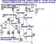
Unfortunately, LTSpice does not render the junction '.' correctly on .wmf output under WINE/Linux. Every place where a line crosses another at 90 degrees has a junction, except where I specifically kink it with a '-_-' to indicate that there's no junction (there's one such dog-leg in this schematic).
To understand it better, consider the topology to consist of two separate halves - Q1 & Q2 form the first half, a simple non-inverting voltage amplifier, and Q3, Q4 and Q5 form a unity-gain voltage buffer for the signal at the collector of Q2 (that buffer is a simplified BJT version of a clever JFET buffer from Steven/MikeB). An emitter-coupled voltage-series feedback network consisting of R5 and R6 sets the closed-loop gain of ~10.
The main change in this schematic from its predecessor:
http://www.diyaudio.com/forums/showthread.php?postid=1576537#post1576537
is that the bootstrap for the collector load (R7) of Q2 has been simplified. I just directly hook R7 to the emitter of voltage follower Q4, taking advantage of the property that Vbe of Q4 stays fairly constant (that's one advantage of the Steven/MikeB voltage follower, where they use a JFET with Vds, Id and Vgs remaining more or less constant. I use a BJT where Vce and Vbe are fairly constant, but Ic varies a bit since I've replaced the current source in the Steven/MikeB buffer with a simple resistor R9).
The net result is that this topology is almost as simple as Elvee's 3-BJT topology (or my subsequent 4-BJT modification), but without an electrolytic cap in the bootstrap path - a big bonus, because that is a significant source of distortion in practice. I still have electrolytics at the input, output and feedback network, but their contributions to distortion can be mitigated with high-quality electrolytics bypassed by suitable film caps.
thanks for clarify, linuxguru
I will re-draw my downloaded image of your circuit
and try to explore it further
lineup
http://lineupaudio.freehostia.com/forum/index.php
I will re-draw my downloaded image of your circuit
and try to explore it further
lineup
http://lineupaudio.freehostia.com/forum/index.php
OK, here's a further improvement on the same topology. The main changes are:
1) A shunt feedback resistor (R11) has been added from the collector to base of Q3 & Q5, thus linearizing the output buffer (Q3-Q4-Q5). The bonus is that it is driven from the low-impedance node at the emitter of Q4, so we don't lose much by way of gain for Q3 & Q5.
2) The second bonus is that this allows the removal of the Miller capacitor (C4 in previous schematic) for Q3 & Q5 without loss of stability.
3) The Miller capacitor C3 for VAS Q2 has been increased to 180 pF - not for stability, but for increased VAS linearity.
4) The changes allow the use of commodity 2sc1815 (Q1) for the input stage, and 2sa1015 (Q3) in the output buffer, lowering costs. 2sa992/2sa970 is retained for the VAS (Q2).
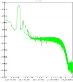
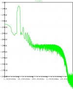
The net result is that THD20 is now improved, with simulated H2 less than -100 dB at 1.5 mW into 32 ohms. At 0.15 mW, H2 is now ~ -120 dB (0.0001%). In both cases, H2 is greater than H3 by 20 dB or greater. Quiescent current is slightly higher at ~16.5 mA at Vs=3V.
With the THD20 now down below the -100 dB range, premium electrolytics like Cerafine or Silmic II are indicated for the input coupling cap C1 in a typical implementation. The output coupling cap can be any low-ESR audio-grade cap like Panasonic FC or Rubycon ZL.
1) A shunt feedback resistor (R11) has been added from the collector to base of Q3 & Q5, thus linearizing the output buffer (Q3-Q4-Q5). The bonus is that it is driven from the low-impedance node at the emitter of Q4, so we don't lose much by way of gain for Q3 & Q5.
2) The second bonus is that this allows the removal of the Miller capacitor (C4 in previous schematic) for Q3 & Q5 without loss of stability.
3) The Miller capacitor C3 for VAS Q2 has been increased to 180 pF - not for stability, but for increased VAS linearity.
4) The changes allow the use of commodity 2sc1815 (Q1) for the input stage, and 2sa1015 (Q3) in the output buffer, lowering costs. 2sa992/2sa970 is retained for the VAS (Q2).
The net result is that THD20 is now improved, with simulated H2 less than -100 dB at 1.5 mW into 32 ohms. At 0.15 mW, H2 is now ~ -120 dB (0.0001%). In both cases, H2 is greater than H3 by 20 dB or greater. Quiescent current is slightly higher at ~16.5 mA at Vs=3V.
With the THD20 now down below the -100 dB range, premium electrolytics like Cerafine or Silmic II are indicated for the input coupling cap C1 in a typical implementation. The output coupling cap can be any low-ESR audio-grade cap like Panasonic FC or Rubycon ZL.
Attachments
- Status
- Not open for further replies.
- Home
- Amplifiers
- Headphone Systems
- Five-BJT low power headphone amp