Resistance in test leads? In the old days, you could set the analog meter to zero with the leads shorted together.
Use a 4-terminal measurement for low resistances, otherwise you may be simply seeing contact resistance of the connections between the board and multimeter innards. Normally anything under 1 ohm is highly unreliable with a multimeter. Not that 200 milliohms is unreasonable for standard PCB really (0.035mm thick traces have appreciable resistance if long/narrow).(out of curiousity, I checked with a multimeter and it reads 0.2 R between the two grounds, so it's not a direct connection)
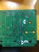
More simplification, added a front copper pour and pad/thermal vias for the submini tubes.
Those via's and copper pours won't be providing any thermal reduction for Valves/Tubes. There is limited thermal coupling from the submini tube to the copper pour. Proper air circulation is the best method to provide cooling - https://audioxpress.com/article/the-internal-life-of-vacuum-tubes
Device packages such as DPAK, SOT223, LFPAK and IC's with thermal pads use copper pours to provide heatsinking. The internal die is thermally and/or electrically connected to the device external thermal pad or footprint.
Did you already ordered the board?
I'm advising against ground splits. A plain ground plane is always better than anything else, even when you have digital stuff going around. The problem with plane splits is that you are kind of creating antennas on the board.
You need to stitch the top and bottom GND pours with vias, kind of like this:

See how there are free vias all around?
This will ensure that your top and bot planes are very well connected even tho it's cut by signal traces.
Do not follow design guidelines from the tube era, apply the newest techniques. It makes no sens to apply star topology on a multi layer PCB. It was very important when gears were a bunch of wire nailed to a board.
High speed electronics laying around your preamp will wreak havoc on it if it's not designed right. There has been cases of whole recording studios shutting down because of 4G relays. A forensic was conducted and it came to conclusion that the relay was not the issue, it was performing as planned and according to the regulations. The old gears in the studio however...
Current doesn't follow the path of least resistance, it follows the path of least impedance. If you don't provide a convenient, low impedance path for the return current of any signal, congrats, you just made an antenna. You may not emit, but you'll receive. If the return path of an offending signal can couple with the signal trace or return path of a signal, you get crosstalk. You really have to think about where your current will flow.
Watch the Rick Hartley interviews and webinars, it helped me a lot to understand all of this. Good luck 😉
I'm advising against ground splits. A plain ground plane is always better than anything else, even when you have digital stuff going around. The problem with plane splits is that you are kind of creating antennas on the board.
You need to stitch the top and bottom GND pours with vias, kind of like this:
See how there are free vias all around?
This will ensure that your top and bot planes are very well connected even tho it's cut by signal traces.
Do not follow design guidelines from the tube era, apply the newest techniques. It makes no sens to apply star topology on a multi layer PCB. It was very important when gears were a bunch of wire nailed to a board.
High speed electronics laying around your preamp will wreak havoc on it if it's not designed right. There has been cases of whole recording studios shutting down because of 4G relays. A forensic was conducted and it came to conclusion that the relay was not the issue, it was performing as planned and according to the regulations. The old gears in the studio however...
Current doesn't follow the path of least resistance, it follows the path of least impedance. If you don't provide a convenient, low impedance path for the return current of any signal, congrats, you just made an antenna. You may not emit, but you'll receive. If the return path of an offending signal can couple with the signal trace or return path of a signal, you get crosstalk. You really have to think about where your current will flow.
Watch the Rick Hartley interviews and webinars, it helped me a lot to understand all of this. Good luck 😉
Last edited:
Thanks for the tips, but unfortunately I already built it. You're right, it's noisy, but it's good enough for my purposes (need it for a show next weekend). I'm planning a redesign in the next couple months so will ditch the star ground for a modern ground plan. Will check out RIck Hartley's content.
BTW the top and bottom pours are stitched with vias. But probably not enough. The ground is so noisy I can't use it for the ground of the balanced inputs/outputs. Luckily it seems to be fine if I lift it (i.e. disconnect the XLR ground from circuit ground) and just pass it through. Not ideal, but good enough for a prototype.
But it works! I had a few mistakes - my holes for solder wires were too small. 😀 I had the pin order backwards for the vacuum tubes (I read the schematic as looking from the top instead of from the bottom. My 10dB H-pad was insufficient and the output was too hot. But I managed to work around all of those - surface-mounted the wires, did some creative braiding of the tube leads, swapped out the H-pad for a 30db. And it works basically the same as the simulation!
I'm pretty happy considering it's my first ever design I've built that wasn't a kit. I had a lot of fun simulating it in KiCad and tweaking values and it's very satisfying to see the real world match it.
Thanks to everyone on here for all of your help, I learned a lot.
Attachments
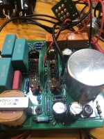

Aha! As I was installing it in an enclosure, I noticed that I had the wiring wrong on the out XLR - I’d swapped shield with one of the balanced outputs. I fixed that and the hum is gone.
The last remaining issue is a faint high-pitched squeal that I’m pretty sure is coming from the boost module. I either need another decoupling cap or a shield.
The last remaining issue is a faint high-pitched squeal that I’m pretty sure is coming from the boost module. I either need another decoupling cap or a shield.
I added a second 10uF decoupling cap to B+ and the whine is gone. And I added a 1M resistor across the input transformer to take care of the audible "click" when switching between active and bypass. <dance of joy>
- Home
- Design & Build
- Construction Tips
- First PCB design, any feedback before I order?