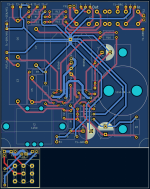
Hey, I've been working on a mic preamp in a stompbox based off this TapeOp article. I swapped out the tubes for Soviet subminiature 6N16Bs and added a H-pad at the end to reduce the voltage back to microphone level. I simulated it in KiCad and tweaked the plate and cathode resistor values until I had something I liked, and also added an L-pad after the second preamp stage to prevent the cathode follower from clipping. Anyway, I've sourced the parts, found a Hammond enclosure, and designed the PCB. I think I've followed all of the rules - 45 degree angles, keep audio and power ground separate, star ground for audio, avoid crossing traces, and if it's unavoidable, have them cross at a 90 degree angle. This is my third PCB design iteration and I think I'm ready to place an order. But before I do, I thought it would be wise to ask for feedback.
K1 and K2 are relays controlled by the footswitch.
T1 is the input trafo, T2 the output trafo.
There are two POT_GNDs because the cables are shielded.
U1 is configured as two cathode-biased preamps, and U2 as a White cathode follower.
The trafos and balanced input and output connect on the bottom of the board.
The footswitch has its own pcb (at the bottom) that I'll cut off. It will stand above the the empty spot at the bottom middle.
C8 is a decoupling cap, the others are all coupling.
The power source is a tiny (25mm x 25 mm) nixie tube power supply. It will sit under the board, below the output trafo. I'm going to add a grounded copper pour under the output trafo to provide some shielding, but if that's not enough, I'll have enough clearance to put a shield between them.
The audio path goes from the balanced input XLR (IP2/IP3) to the input trafo primary (T1-ORG/T1-BRN). The unbalanced secondary (T1-GRN) goes to via the grid stop (R19) to U1, then from U1 to POT_OUT to a gain pot, then to POT_IN, to C3, back to the second triode in U1, then to R16. That goes directly to the cathode follower U2, which outputs to to C6, then to T2-B (output trafo). Finally, the secondary output (balanced - T2-G/T2-Y) goes through the H-pad at the top left before entering K2 and finally to the output XLR (OP2/OP3).
When the coils of K1 and K2 are disengaged, IP2/3 and OP2/3 are connected directly and the H-pad becomes a dummy load.
Any feedback on my placement and routing? F.Cu is red, B.Cu is blue. All audio ground is routed on B.Cu.
Thanks!
Last edited:
Have you built a hardware prototype yet, or will this board be it?
Generally, a board rev.1 will have enough problems that you'll usually make at least a rev.2.
Have you followed proper creepage and clearance? Looks a little tight around the tubes.
Generally, a board rev.1 will have enough problems that you'll usually make at least a rev.2.
Have you followed proper creepage and clearance? Looks a little tight around the tubes.
It's difficult to tell with no scale, the tracks look a little thin, given its a through hole design the pcb tracks could be wider.
From the image it seems you have two unconnected tracks indicated by the grey line - from U1 to FS3 and U2/FS1 to J23/D1
The clearance of the ground return track around the pad of C6 needs to be increased.
The track starting from U1 and running through U2 to FS1 may need to be re-routed due to clearance issues, you could easily route this on the bottom layer.
Good practice is to ensure you have sufficient clearance between components and pcb tracks from the edge of the pcb. It looks like you have components mounted right on the edge of the pcb.
You could also improve some of the routing by placing pcb tracks on the bottom layer.
Since there are two unconnected pcb tracks, this is an indication you haven't run the DRC to ensure there are no errors on the pcb layout.
From the toolbar goto "inspect " and then select "Design Rules Checker" and click on "Run DRC"
The DRC checks for general errors, including the specific rules you created in the board setup.
You should also run DRC on the schematic to highlight any errors.
Last edited:
Thank you, this is very helpful!
Yes, this is the prototype. I assume there will be a v1.1.
Good point on clearance, thanks - I didn't have sufficient clearance. I have been running DRC, but I didn't have a netclass with appropriate clearance for 150V (0.6mm). I added one and ended up redoing a bunch of work to clear the errors.
The grey lines are aren't a problem. The separate nets are connected by off-board wires. FS1/2/3 are connectors.
I will rerun ERC just to be sure.
I increased the pcb edge clearance to a minimum of 1mm.
As for trace widths, the maximum draw for this circuit (excluding heater & relays) is 5mA. According to this calculator a 0.25mm trace width (which is what I'm using) should be fine up to 100mA.
I have the heater and relays on a completely different circuit, with separate ground. The heaters draw 0.8A total, and I used a trace width of 0.4mm. That should be safe up to 2A.
However, I can't find any information about through-hole vs. surface-mount. Can you explain what you mean by this?
the tracks look a little thin, given its a through hole design the pcb tracks could be wider.
You pay for the copper anyway, so why not use it? 😎
You can get away with thin traces, but that doesn't mean you should. Not only will thicker traces handle more current, they will also better tolerate soldering (and resoldering) without lifting - once you've done a prototype or two you may well be happy about this...
I would size the traces up to something like 40-50 mil (app. 1mm - 1.25mm) as the standard for the entire board and then reduce the size if it is required - you seem to be thinking the other way around, i.e. start small and size up where absolutely necessary.

But why push the process? You're not pressed for space. My standard "low current" trace width is 12 mil (0.3 mm). For stuff that draws current, I up it to 20 mil (0.5 mm). I'd probably use 20-40 mil wide traces for the heaters. You pay for the copper anyway.As for trace widths, the maximum draw for this circuit (excluding heater & relays) is 5mA. According to this calculator a 0.25mm trace width (which is what I'm using) should be fine up to 100mA.
I have the heater and relays on a completely different circuit, with separate ground. The heaters draw 0.8A total, and I used a trace width of 0.4mm. That should be safe up to 2A.
With skinnier traces and tighter spaces you're more likely to have production issues. I'm guessing you're not planning to pay for electrical testing of the boards before they ship from the manufacturer, so it makes sense to be a bit conservative on the design rules. I've had production issues on boards with 12/12 mil trace/space even with a quality manufacturer like OSH Park. Sometimes stuff happens, especially on shared board runs.
I tend to keep traces at least 50 mil (1.3 mm) away from board edges. I keep component pins at least 100 mil (2.54 mm) away from the board edge, preferably 150 mil (3.8 mm).
Also: Don't forget to add mounting holes. I add a 130-mil (3.3 mm) hole, 200 mil (5.08 mm) away from each corner of the board. That works well with M3 machine screws.
Tom
I would increase the pcb edge clearance to at least 2mm unless there is some specific requirement to do so.
PCB track width is more important for high current tracks or where impedance is to be considered (transmission line/microstrip). There's no need to calculate track widths and scale proportionately for such low currents.
You would only use thin pcb tracks where restrictive routing or spacing is required. This is not normally an issue when using through hole components as there is plenty of pcb real estate to route tracks around.
When using 0.25mm tracks you need to consider how well these will stand up to handsoldering (mechanical resilience). When using SMT everything is much smaller including the connecting pcb tracks.
Given the amount of free space and every component is through hole I would consider a minimum track width of 1mm. Where routing or clearance is an issue utilise the bottom layer to move around obstacles and use via's to connect the top and bottom tracks.
The calculator you're using for pcb track current is obsolete. IPC2221 has been replaced by IPC2152. You can download a excellent pcb tool calculator from Saturn PCB Design - https://saturnpcb.com/saturn-pcb-toolkit/
Untangling the ratsnest can be one of the hardest parts. And it can be an iterative process. You've already got a star ground, but a ground plane would probably be better to reduce RFI. But once you have a plane in place, it may be possible to shorten many of the other tracks with little or no penalty to the performance of the ground.
The solder pad for B+ is under a capacitor. What's the plan there?
Same question for the connections under the two relays. If you intend to solder wire to those you'll likely find that a slight tug on the wire will peel the pad and trace right off. If that happens while the amp is on you could have B+ connecting to places where you really don't want it.
Bring those out to a suitable connector or terminal block located along the board edge.
It looks like you have silk screen on both sides of the board. Beware that many prototype PCB places only gives you silk screen legend on one side.
Tom
I'd add to be mindful of heat generators and their proximity to other components. Particularly in the case of electrolytic caps, I keep them away from any high power resistors and such.
So in your case, the proximity of the tubes to the capacitors - U1/C1, U2/C6.
I default to 0.8-1mm signal traces and 1-1.5mm power traces depending on routing space, and reduce size as necessary. I tend to lay out for the shortest ground routes and avoid loops, then use a ground pour with notches cut as necessary to divide up the power / signal grounds for a single return point.
I second (or maybe third or fourth) leaving edge distance. I personally go for 5mm either edge when I use the Hammond extruded cases where I want to slide the PCB in. It is too easy to get a component either mechanically interfere with the case, or worse still, have a heap of solder tails short out 🤦♂️
PCB layout is definitely an iterative process. I often get a layout done, then start again from scratch and see if I can come up with another way. My OCD also forces me to make the layout as symmetrical as possible...
Thank you everyone, looks like I'm on to my next iteration. 🙂
Saturn PCB is giving me a 404, but I found an IPC2152 calculator here: https://ninja-calc.mbedded.ninja/calculators/electronics/pcb-design/track-current-ipc2152
But... it sounds like minimum trace width is much less relevant than practical considerations for through-hole, so I will bump up my trace widths as recommended.
Minimum trace width is just that - a minimum. If you have the space, make use of the copper that you've paid for. If space is tight, reduce the widths as necessary but not below the minimum.
For example, you could get away with a minimum 0.9mm track width to run 5 amps, but the track will heat up 40 degrees (Celsius) above ambient.
Make that same track 2mm wide and it only rises 16 above ambient. That will be more reliable.
High speed / frequency circuits are a little different in that you need to impedance control and match data lines (for example), but for audio stuff in the low KHz range, that's not really so relevant.
And as others have pointed out, tiny tracks are more prone to lifting when soldering/desoldering/resoldering as inevitably happens in the prototype stage.
Another tip if using ground pours - make sure that ground pads are connected via Spokes - this will help avoid dry joints. Without spokes, you end up having to heat up the entire ground plane to get the solder to stick whereas with spokes, you get a little thermal break between the copper mass and the pad.
Am interested to see your next version when you are ready.
Yep. Definitely use thermal reliefs on pours.Another tip if using ground pours - make sure that ground pads are connected via Spokes - this will help avoid dry joints.
Tom
Next iteration. The subminiature tubes are connected by leads, not sockets, so I got creative with pin spacing in order to fit everything.
Trace widths are 1.5mm for filament & relay coils, 1mm for everything else. Clearance is 0.6mm for high voltage (150V at B+) and 0.3mm for everything else. I might have missed some HV nets, will do a pass on that as well.
Edge clearance to components is 5mm, though I had to place the solder pads and the bottom bit of T2 within that to make everything fit. No vias. Grounds are as consolidated as possible - each cathode has its own ground, as do trafos, L-Pad and XLR shields.
The ground pour is connected to PWRGND in one spot (near the board centre) with thermal relief spokes.
Attachments
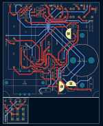
More simplification, added a front copper pour and pad/thermal vias for the submini tubes. Also rerouted some high-voltage traces to avoid other signal traces. Also added more clearance around the trafo through-holes to avoid the nuts damaging the copper. I think I'm done?

It looks like you have separate ground traces and ground plane on the back layer. Is there a reason for not incorporating the ground traces into the ground plane? Perhaps, an image showing just the back layer would make things more clear.
That's correct. There are two circuits - the 12 V relay coil and tube heaters, and the 150V audio. The boost board I'm using to get 150V has separate grounds for 12V and 150V (I called them PWRGND and GND), so I opted to keep those separate in my design. The front and back both have ground planes connected to PWRGND, except for a small blob where the GND traces connect. Everything I've read about tube circuits recommends a star ground topology (or at the very least separated ground planes) to avoid ground loops, so that's what I did.
Here's front and back views - I've iterated a bit more since the last screenshots:


Here's front and back views - I've iterated a bit more since the last screenshots:
Last edited:
- Home
- Design & Build
- Construction Tips
- First PCB design, any feedback before I order?