Hi all, looking for some advice on PCB layout, and improvements, it's my first attempt at a 2 layer PCB.
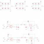
The following is for the IV stage and output for a Denon DCD820 2x PCM56P-L +/-1ma.
After reading the threads I have opted for the OPA861 with the LM6172 as the buffer, as it can deliver a high current if needed.
I've run the simulation in Tina and LTSpice, all looks good. C5/8 & R9/10 are there because the lm6172 requires them in unity gain mode.
I've done a fair amount of research watched quite a few video lectures including Altium and Cadence.
One of the key points was to try and get all the traces on one side and use the other for GND with a clear unbroken signal return path.
I know it may need local voltage regulators depending on where I take the power from, as this CD has a +/- 10V and +/-5V both used on the analogue circuits.
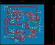
The power rails are 50mils and the signal is 24mil. I'm not happy with the top left as it is not too neet.
Thanks, Tom
The following is for the IV stage and output for a Denon DCD820 2x PCM56P-L +/-1ma.
After reading the threads I have opted for the OPA861 with the LM6172 as the buffer, as it can deliver a high current if needed.
I've run the simulation in Tina and LTSpice, all looks good. C5/8 & R9/10 are there because the lm6172 requires them in unity gain mode.
I've done a fair amount of research watched quite a few video lectures including Altium and Cadence.
One of the key points was to try and get all the traces on one side and use the other for GND with a clear unbroken signal return path.
I know it may need local voltage regulators depending on where I take the power from, as this CD has a +/- 10V and +/-5V both used on the analogue circuits.
The power rails are 50mils and the signal is 24mil. I'm not happy with the top left as it is not too neet.
Thanks, Tom
Attachments
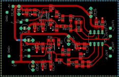
Kinda hard to see, but looks ok for a first effort, and is a good basic approach.
A couple of hints:
Place all the nfb components first, to minimize the high impedance node area (inverting input).
Don't like the unterminated emitter inputs. Add resistors to ground, around 20 times
the emitter input impedance.
If possible, use an identical layout for the L and R, at least up to the shared output package.
Can't tell if they are there, but be sure to use thermal reliefs on pads to the ground plane.
Last edited:
Hi rayma thanks for the advice, I shall give those ideas ago.
I've added some, hopefully, better images.
To make it clearer I left out the ground plane which is pretty solid apart from the through-hole components and the vias.
The terminal reliefs are there and set to 24mil.
Thanks for pointing out the unconnected pins; I've just read the TI paper on unused opamps in multi op-amp devices.
The two pins, 5 and 6, on the OPA861 are not connected according to the datasheet. Does this make a difference?
Attachments
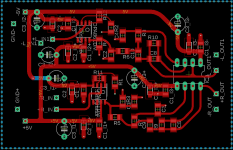


For an unused op amp, connect its output to the inverting input, and also connect the non-inverting input to ground.
For a single supply circuit, connect the non-inverting input to the Vcc/2 bias point.
However for the OPA861, pins #5 and #6 are no connect.
Move both R1 and R2 down and left, so they are each horizontal, and between the input trace and the supply bypass capacitors.
For a single supply circuit, connect the non-inverting input to the Vcc/2 bias point.
However for the OPA861, pins #5 and #6 are no connect.
Move both R1 and R2 down and left, so they are each horizontal, and between the input trace and the supply bypass capacitors.
Last edited:
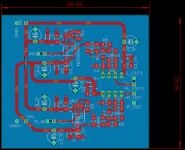
Seems ok now, if the net connects all the right pins to all the right places.
I usually print it out in a large size and trace each connection out with a marker to verify
its connected the same as the schematic.
I usually print it out in a large size and trace each connection out with a marker to verify
its connected the same as the schematic.
Believe me, it is. Don't ask how I know.Thanks for the help and the reply. Tracing out seems like a good idea too.
Print it as large as possible, and then use a color marker to trace out all of the connections to each of the circuit nodes,
one at a time. Do the same on the schematic, and make sure that they match.
Then check the IC footprints compared to the data sheet, all capacitor polarities, and the connector pinouts.
You cannot be too careful and methodical, even on a simple board. A popular error to make is using the
bottom view of a relay or IC as the top view instead, so all the pins are wrong. Pins are always numbered CCW
as viewed from the top.
Last edited:
- Home
- Source & Line
- Digital Source
- First PCB attempt