I'm fixing a Fender Acoustasonic SFX II guitar and PA amp for a friend. I found that the 4 output transistors in this amp (there are 2) basically just cook like crazy. They get extremely hot very quickly even with no signal input, but the DC voltages at the test points check out fine. Nothing looks bad on the board. The power supplies appear to be ok. I took the main board out and these 4 outputs have been replaced before, as well as a small temperature responsive part. It's obvious from the soldering what's been replaced.
So, I put this amp into my simulation software and it appears that the outputs are supposed to operate in class B, since the quiescent current in each output models at less than 1mA. Is this normal for Fender guitar amps?
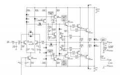
I'm having a little trouble figuring out the stuff between the input differential pair and the drivers. It looks to me that the 2.43k resistor sets the bias in the output transistors. I was wondering if the emitter resistors in the outputs was too low (0.15 ohms). I doubled them in the simulation and the distortion went down. I think it would be a good idea to increase the emitter resistors to help protect the outputs.
Also, if the test points check out for DC voltages, can I assume that everything up to the drivers Q26 and Q28 are ok? I was going to take out the drivers and the outputs and test them. Is there a way to check transistors while they are in circuit? I have a DMM with diode and transistor tester functions. I also have a scope and oscillator.
Oh, the 1k resistor R232 in the CCS for the LTP goes to a -34 supply. I didn't check to see if that was working ok, but assumed so because the test points measured fine.
Any suggestions are appreciated.
So, I put this amp into my simulation software and it appears that the outputs are supposed to operate in class B, since the quiescent current in each output models at less than 1mA. Is this normal for Fender guitar amps?
I'm having a little trouble figuring out the stuff between the input differential pair and the drivers. It looks to me that the 2.43k resistor sets the bias in the output transistors. I was wondering if the emitter resistors in the outputs was too low (0.15 ohms). I doubled them in the simulation and the distortion went down. I think it would be a good idea to increase the emitter resistors to help protect the outputs.
Also, if the test points check out for DC voltages, can I assume that everything up to the drivers Q26 and Q28 are ok? I was going to take out the drivers and the outputs and test them. Is there a way to check transistors while they are in circuit? I have a DMM with diode and transistor tester functions. I also have a scope and oscillator.
Oh, the 1k resistor R232 in the CCS for the LTP goes to a -34 supply. I didn't check to see if that was working ok, but assumed so because the test points measured fine.
Any suggestions are appreciated.
Attachments
One side of the output emitter followers was drawing over 500mA, and the other side was drawing about 166mA.
I did a basic in circuit diode test on the outputs and drivers and the seem ok. The bias setting resistors are in spec as well, and the Vbe multiplier Q16 tests good in circuit as well.
I'm stumped. I don't know why the output current draw would be unbalanced, and I don't know why they draw so much current when the DC test points check out OK. The loudspeakers were disconnected for these tests.
Short out the Vbe multiplier (collector to emitter) this will reduce bias to zero, if this stops it getting hot, then you need to make it adjustable. If it doesn't stop it getting hot, then you have a fault.
Generally it's pretty rare for just the output devices to fail, so if only those were changed perhaps the actual fault wasn't cured - and it's simply frying the new transistors as well.
Generally it's pretty rare for just the output devices to fail, so if only those were changed perhaps the actual fault wasn't cured - and it's simply frying the new transistors as well.
Short out the Vbe multiplier (collector to emitter) this will reduce bias to zero, if this stops it getting hot, then you need to make it adjustable. If it doesn't stop it getting hot, then you have a fault.
Generally it's pretty rare for just the output devices to fail, so if only those were changed perhaps the actual fault wasn't cured - and it's simply frying the new transistors as well.
OK, great. Thanks for the suggestion. I'll try that. The Vbe multiplier is I guess Q16, which is a funny little transistor mounted right next to the heat sink. I tested it in circuit with the diode tester and it seems to be OK.
I do suspect that the actual fault was not repaired.
It would be easier to jumper the 2.43K and 33 ohm resistors. In the sim it has the same effect of shutting off the outputs. It's really hard to jumper Q16 without soldering. I think I'll try that.
Or short the collectors of Q18 and Q20 together, exact same points - you don't need to do it on the actual Vbe multiplier.
Shorting the resistors isn't quite the same, and doesn't prove if the Vbe multiplier is duff.
Incidentally - the amp (assuming nothing else is duff) will work pretty well with the bias at zero, as long as you play it loud - perfect guitar amp! 😛
Shorting the resistors isn't quite the same, and doesn't prove if the Vbe multiplier is duff.
Incidentally - the amp (assuming nothing else is duff) will work pretty well with the bias at zero, as long as you play it loud - perfect guitar amp! 😛
Hi,
I'm confused, there is nowhere for your unbalanced currents to go.
Have you checked the DC voltages across all the output resistors ?
And checked there should be ~ 0.6V across all transistor base/emitters ?
(except of course for the protection transistors ...)
What DC voltage across the Vbe multiplier do you sim and measure ?
0.15R for the emitter resistors should be fine, no need to double.
rgds, sreten.
Hi,
I'm confused, there is nowhere for your unbalanced currents to go.
Have you checked the DC voltages across all the output resistors ?
And checked there should be ~ 0.65V across all transistor base/emitters ?
(except of course for the protection transistors ...)
What DC voltage across the Vbe multiplier do you sim and measure ?
This minus 2 Vbe drops should be the voltage across R248.
Similarly R248 voltage minus 2 Vbe drops determines the voltage
across the emitter resistors and hence the standing bias current.
0.15R for the emitter resistors should be fine, no need to double.
rgds, sreten.
Hi,
I'm confused, there is nowhere for your unbalanced currents to go.
Have you checked the DC voltages across all the output resistors ?
And checked there should be ~ 0.6V across all transistor base/emitters ?
(except of course for the protection transistors ...)
What DC voltage across the Vbe multiplier do you sim and measure ?
0.15R for the emitter resistors should be fine, no need to double.
rgds, sreten.
Thanks for your help. In the sim I measure -1.48 on the emitter of Q16 (the Vbe multiplier) and +1.4V on the collector. I can measure it in real life later.
I have to put the board back in the amp to test it with power. I was just concerned that something would smoke if I left it on very long so I thought I'd try testing parts with it out.
The voltages across the emitter resistors in the finals were unbalanced. One side had I think 75mV and the other about 25mV across 0.15ohms. That was a head scratcher for sure, since no speaker or other load was attached to the output.
I didn't check the voltages across the base/emitters in the finals because I didn't have the data sheet with me so I didn't know which pin was what. Now I do so that's a good test. thanks.
OK, I shorted Q16 and that shut off the outputs completely. They remained ice cold and there was zero voltage across each of the emitter resistors. Does this mean that Q16 is bad? I guess the definitive test will be to remove it and test it then. I also checked the negative DC voltage for the CCS on the LTP and it was correct (-36VDC @ R232).
Thanks again for the help.
I removed the jumper and measured 2.5V across Q16, Vce.
While it was on, I also measured the Vbe for each output and the two drivers. All were about 0.6V (+ or-).
Thanks again for the help.
I removed the jumper and measured 2.5V across Q16, Vce.
While it was on, I also measured the Vbe for each output and the two drivers. All were about 0.6V (+ or-).
Last edited:
SHorting Q16 is supposed to turn off the outputs. That they were overheating before doesn;t mean that Q16 must be faulty, though it could be. What the test shows is that your outputs and drivers are not sitting there leaking.
Those TO218/247/TO3P type transistors as used for outputs all have the same pinout: base, collector, emitter, left to right across the front.
You may be comfortable with it, but to me, using a simulation for troubleshooting is asking for confusion.
If there is a current difference between sides, did you measure across ALL the emitter ballast resistors? Or just one per side, assuming the other on each side to be the same?
Certainly any offset from zero on the output would send current through a load, but just having both sides conducting will also cause current to flow. If they are not equal, then what if one output of the pair on a side is not conducting, but both opposing ones qare. Then the current on the faulty side would all flow through one transistor, but when it goes through the other side it will be shard by the two. So the current through the one emitter would be twice that through each in the working pair. Just a thought. No load involved.
Did you check ALL those fusible 4.7 ohm base resistors on the outputs? Are any of those 0.15 ohm emitter ballasts open?
It is good to want to find a bad part, but an open resistor can be just as bad as a bad transistor. Same with a cracked solder joint or cracked pc trace. Change transistors all day and those things won;t be solved.
Please don;t modify the circuit - don;t change the emitter resistors. The problem is a circuit failure, not a design flaw. If those resistors needed to be changed, then ALL the Acoustasonics out there would be burning up. And they are not.
Testing transistors, at least using a hand meter, is a gross measurement. The diode test approach tells you the transistor basically acts like a transistor. That test will reveal shorted or open ones and other gross failures. WHat that test won't reveal is a part that leaks at voltage, or can;t amplify well, or any number of other conditions. Basically it will show bad parts but won;t guarantee they are good parts.
R248 between the driver emitters, is it on value?
The schematic calls for 2.3v between driver bases, you have 2.5, a little high.
If you do need to adjust the bias, reducing R250 or increasing R254 would tend to reduce idle current through the outputs.
It is unclear to me from your description. Are BOTH amplifiers overheating, or just the one we are discussing?
I removed the jumper and measured 2.5V across Q16, Vce.
While it was on, I also measured the Vbe for each output and the two drivers. All were about 0.6V (+ or-).
Hi,
Well that means your left with 100mV across 0.15R, i.e. 666mA bias current !
The bias voltage is a little high. What you want is about 25mV across
each emitter resistor, this gives about 300mA total bias current.
If you double the emitter resistor values the optimum bias voltage
does not change, the optimum bias current becomes ~ 150mA.
rgds, sreten.
In this case though there not much harm in underbiasing it .....
Last edited:
I'm not happy about a amp having fixed bias - and in this case I'm pretty sure it doesn't.
R250 probably isn't 2.43K it's more likely ' 2 - 4.3K' - the actual value is selected during final inspection at the factory, and a fixed value fitted (poor design!).
I would replace R250 with a 4.7K preset resistor, adjust it to zero ohms, then power the amp up and gradually turn the bias up whilst monitoring it.
I agree with the others that it would be EXTREMELY stupid to mess about with emitter resistor values, which would have next to no effect anyway (they aren't terribly crucial). I'm also bemused by running a simlator?, I don't see how it helps in any way?.
The voltages across the emitter resistors in the finals were unbalanced.
One side had I think 75mV and the other about 25mV across 0.15ohms.
Hi,
This could be bad soldering and/or dodgy resistors. What it would tell
me for a single output pair is one resistor is 3 times the value of
the other. But you have two pairs and need to measure all
4 emitter voltages and check their values.
It is not EXTREMELY stupid to change emitter resistor values at
all as long as you remain in a reasonable range. If bias thermal
stability is a concern the common values of 0.22R or 0.33R can
used and there is absolutely nothing wrong with doing this.
rgds, sreten.
SHorting Q16 is supposed to turn off the outputs. That they were overheating before doesn;t mean that Q16 must be faulty, though it could be. What the test shows is that your outputs and drivers are not sitting there leaking.
Those TO218/247/TO3P type transistors as used for outputs all have the same pinout: base, collector, emitter, left to right across the front.
You may be comfortable with it, but to me, using a simulation for troubleshooting is asking for confusion.
I wasn't using the sim to troubleshoot. I was using it to try to understand the circuit. I'm not as knowledgeable as you about these things. I can't just look at it and say "ah, this does that", at least not yet. I'm getting better though.
It is not EXTREMELY stupid to change emitter resistor values at
all as long as you remain in a reasonable range.
It is if the reason for doing it is to try and reduce too high a bias current 😀
Like I also said, their value its very non-critical.
It is if the reason for doing it is to try and reduce too high a bias current 😀
Like I also said, their value its very non-critical.
Well, this is where the sim is handy. Increasing the emitter resistors reduces distortion in the sim. So, there's a reason to do it, but I'm not planning on doing that now. I need to find the bad part and replace it.
The bias is fixed at the factory. That really is a 2.43k 1% resistor in there. I measured them. They don't twiddle with the values to fine tune it. Fender is not what I would call high quality.
I will check the bias in the finals again. What was happening the last time was that the values were moving higher and I got concerned so I shut it off. When I have time I can give a time vs. voltage thing. The finals don't immediately overheat. They sit there for a while and slowly start to get hotter and hotter.
The owner says it plays fine for a while, then after a while it starts to sound bad.
Did you check ALL those fusible 4.7 ohm base resistors on the outputs? Are any of those 0.15 ohm emitter ballasts open?
It is good to want to find a bad part, but an open resistor can be just as bad as a bad transistor. Same with a cracked solder joint or cracked pc trace. Change transistors all day and those things won;t be solved.
Please don;t modify the circuit - don;t change the emitter resistors. The problem is a circuit failure, not a design flaw. If those resistors needed to be changed, then ALL the Acoustasonics out there would be burning up. And they are not.
Testing transistors, at least using a hand meter, is a gross measurement. The diode test approach tells you the transistor basically acts like a transistor. That test will reveal shorted or open ones and other gross failures. WHat that test won't reveal is a part that leaks at voltage, or can;t amplify well, or any number of other conditions. Basically it will show bad parts but won;t guarantee they are good parts.
R248 between the driver emitters, is it on value?
The schematic calls for 2.3v between driver bases, you have 2.5, a little high.
If you do need to adjust the bias, reducing R250 or increasing R254 would tend to reduce idle current through the outputs.
It is unclear to me from your description. Are BOTH amplifiers overheating, or just the one we are discussing?
Just one amplifier is overheating.
The design is not that good in my opinion, but I need to repair this first.
Obviously, testing transistors in circuit is a gross test. I didn't want to go unsoldering them.
I didn't measure R248.
If any of the emitter resistors on the finals were open then they wouldn't have behaved the way I tested, which was to show increasing voltage as the amp got hotter and hotter.
Well, this is where the sim is handy. Increasing the emitter resistors reduces distortion in the sim. So, there's a reason to do it, but I'm not planning on doing that now. I need to find the bad part and replace it.
Simulators aren't the 'real world', ands increasing the value of the emitter resistors increases local negative feedback, and 'may' reduce distortion. But it also reduces power output, and the heat wasted in the resistors.
But as it's a guitar amp, why would you want to reduce it's distortion? 😛
The bias is fixed at the factory. That really is a 2.43k 1% resistor in there. I measured them. They don't twiddle with the values to fine tune it. Fender is not what I would call high quality.
I downloaded the original from Fender, and in a decent size it's clearly as you say.
It looks a pretty decent design, but having a fixed bias requires EXACT transistors fitting if you have to replace them - your problem 'may' just be that you didn't get the correct transistors direct from Fender?.
I will check the bias in the finals again. What was happening the last time was that the values were moving higher and I got concerned so I shut it off. When I have time I can give a time vs. voltage thing. The finals don't immediately overheat. They sit there for a while and slowly start to get hotter and hotter.
This is called 'thermal runaway', and happens if the bias is set too high.
As I said, replace the 2.43K with a preset (2.7K would be fine), and adjust for similar bias to the good channel. See what happens then.
You could always stick a preset in parallel with the 2.43K if it's easier?.
I downloaded the original from Fender, and in a decent size it's clearly as you say.
It looks a pretty decent design, but having a fixed bias requires EXACT transistors fitting if you have to replace them - your problem 'may' just be that you didn't get the correct transistors direct from Fender?.
This is called 'thermal runaway', and happens if the bias is set too high.
As I said, replace the 2.43K with a preset (2.7K would be fine), and adjust for similar bias to the good channel. See what happens then.
You could always stick a preset in parallel with the 2.43K if it's easier?.
I did not replace the output transistors. Someone else did that before I got it. They are obsolete items anyway.
Maybe I should replace the 2.43k resistor with a trim pot?
- Status
- Not open for further replies.
- Home
- Live Sound
- Instruments and Amps
- Fender Acoustasonic needs help