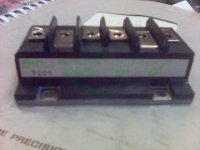
I do not have the datasheets. Maybe a search on google might yield something. From memory I can tell you they were 180vce, 15A, 150watt devices. I have heard guys run these on 250vce rails! I know I upped the rails on an Adcom 555 to +/- 100vdc and ran a 8 ohm load without blowing anything.. (Try it at your own risk, I would NOT recommend anyone do it. 😉 )
Also I 'd like to sell them pairs only otherwise I will be left with mismatched number of PNP/NPN.
If you are interested, I will email you prices,
regards,
PS: I have these on ebay if you like the MJ2119596.
http://cgi.ebay.com/ws/eBayISAPI.dll?ViewItem&item=3830551673&ssPageName=ADME:B:EOAS:US:3
Also I 'd like to sell them pairs only otherwise I will be left with mismatched number of PNP/NPN.
If you are interested, I will email you prices,
regards,
PS: I have these on ebay if you like the MJ2119596.
http://cgi.ebay.com/ws/eBayISAPI.dll?ViewItem&item=3830551673&ssPageName=ADME:B:EOAS:US:3
I have just bought a pair of 2SA1227/? (forgot)😀
Slone used 2SD669/2SB649 in his design. I viewed its datasheet. 2SD669/2SB649 is not linearity but has a high fT .With 2SD669/2SB649 , BW is 30 khz . With 2SA1013/2SC2383,these are quite linearity and fT is only 10Mhz but BW of my amp is 100khz.
The sim is also very good if you use 2SC1775 for VAS and pre driver but I can't use these for VAS and pre driver because heat will destroy these
Easyamp said:Thankyou for all your input, the amp works well as a test bed I never built one like this past the proto board.
I chose the this setup just so that I could get away without having a bias tracking transistor, to ease in swapping out power bjt's and heatsinks and what not.
I varied the bias resistor to acheive roughly 80~100ma between the power bjt's collectors before listening.
You don't need thermal compensation with a Sziklai pair, well at least not for the output stage.
Cheers
Hy Easy,
You need thermal compensation with the CFP output! Especially if the drivers use same heatsink as the output device. I guess to use BJT based bias circuit to avoid the thermal runaway, which will be there!
sajti
K-amps said:I do not have the datasheets. Maybe a search on google might yield something. From memory I can tell you they were 180vce, 15A, 150watt devices. I have heard guys run these on 250vce rails! I know I upped the rails on an Adcom 555 to +/- 100vdc and ran a 8 ohm load without blowing anything.. (Try it at your own risk, I would NOT recommend anyone do it. 😉 )
Also I 'd like to sell them pairs only otherwise I will be left with mismatched number of PNP/NPN.
If you are interested, I will email you prices,
regards,
PS: I have these on ebay if you like the MJ2119596.
http://cgi.ebay.com/ws/eBayISAPI.dll?ViewItem&item=3830551673&ssPageName=ADME:B:EOAS:US:3
I don't think I want pairs at this point. I haven't completely decided what the best approach is. I had planned on using a plastic case (like TO-220 or similar) for the PNP driver (SE class A) and a TO-3 NPN device for the output device. If I Use a TO-3 for the driver as well it will have to mount on the heatsink too I suspose and then I run out of room.
I am also considering paralleling two plastic case devices for the output to keep the current in the most linear range of hfe. However; That 21196 looks like a very nice device. It seems to have a very constant hfe up to 3A or so and I had planned on idling at 1.5A so a single one of those might be just the ticket. The hfe is not very high but if I can find a suitable driver with reasonable hfe it might work out fine.
Another possibility is to use a PNP to drive an NPN darlington device but I have yet to find a darlington that has anything close to constange hfe at any current.
In Nelson's original Adcom 555 design, he drove 4 2sd424's with a single MJE15030/31 I think. Tells me the 424/554's have pretty good Hfe (not as good as the 1302 variants) but good. The 21195/96 are based on the same licensed technology from Toshiba (Perforated emiiter) as the 424/554 parts. This is a step up from the older 15024/25 power base technology which had lower hfe and lower SOAR than the 21195/96.
Good luck! 🙂
Good luck! 🙂
Instead of just guessing, or giving opinions, I suggest that you LOOK UP the different output transistors and get the engineering data sheet on each one. Then, plot on a separate piece of graph paper, the BETA LINEARITY with current, on a LINEAR vs LINEAR plot, which is different from the LOG vs LOG plot that is normally presented with the engineering data sheet. Just overlay the different transistors with a common beta at one specific current, then note which are more linear. F(t) or intrinsic speed is important too! Third, plot the SAFE AREA of each device at some common time constant, like 10ms. This way, you find the most 'rugged' devices when you must have it, in order to keep the amp from blowing up.
john curl said:Instead of just guessing, or giving opinions, I suggest that you LOOK UP the different output transistors and get the engineering data sheet on each one. Then, plot on a separate piece of graph paper, the BETA LINEARITY with current, on a LINEAR vs LINEAR plot, which is different from the LOG vs LOG plot that is normally presented with the engineering data sheet. Just overlay the different transistors with a common beta at one specific current, then note which are more linear. F(t) or intrinsic speed is important too! Third, plot the SAFE AREA of each device at some common time constant, like 10ms. This way, you find the most 'rugged' devices when you must have it, in order to keep the amp from blowing up.
I have been trying to find as much information as I can. I have downloaded quite a few data sheets. On the datasheets that have hfe v.s. current plots I have paid particular attention to that and the SOA. The difficult part is that it is like finding a needle in a haystack to search through thousands of PDF files (on dialup) to locate suitable candidates for further study.
I hadn't thought about graphing hfe on a linear plot for comparison purposes - good idea. Of course I would have to read values off the log plots (for those devices that bother to give that data in the first place) but it sounds like it would be worth the trouble.
What we have here is a curse of riches. With thousands of devices to choose from it is a big task. Thats why I was trying to get ideas of which ones to look at. I have already gotten a lot of good information.
Friendly advice for a fellow Hoosier...
Go with TOSHIBA A1943/C5200 from Digikey. They stock genuine parts. ( even though you could get the hop-ups the A1987/C5359 but you'd be taking a chance. )
Up to 7A they have excellent hfe stability. Self has done some Analysis on load invariant OP devices and he was pretty happy with these. So was Slone and others. This is a good starting point.
Cheers!
Hi, Mr Curl,
I wanted to ask about darlington output stage. In your design you use mosfet for the driver and bipolars as final outputs.
What is the advantage of this configuration, compared to bipolar drivers and bipolar outputs? Or maybe triple darlington bipolar output stage?
I wanted to know the difference, especially audible difference (from your years of experience)
I use a mos fet driver stage, because it presents a high input impedance to the pre-driver stage. This avoids modulation of the open loop gain by changes in the impedance of the loudspeaker load.
I don't like to use mosfets in class AB amplifiers. I think they are very good for high current class A follower application.
To avoid mosfets, I use triple darlington stage, with predriver, and driver in class A. This results high input impedance. To kill the modulation caused by the load, I apply resistors from the base of the predrivers to the ground. This solution decrease the output impedance of the whole amplifier without large feedback, and increase the HF rolloff point between the VAS, and the predrivers. This resistors define the gain for the VAS stage (with the emitter resistor), so I can set the nfb easily.
sajti
That is similar to what I have been doing but without the darlington setup.sajti said:I don't like to use mosfets in class AB amplifiers. I think they are very good for high current class A follower application.
To avoid mosfets, I use triple darlington stage, with predriver, and driver in class A. This results high input impedance. To kill the modulation caused by the load, I apply resistors from the base of the predrivers to the ground. This solution decrease the output impedance of the whole amplifier without large feedback, and increase the HF rolloff point between the VAS, and the predrivers. This resistors define the gain for the VAS stage (with the emitter resistor), so I can set the nfb easily.
sajti
I've only just found this thread and was reading through. I notice that most of the mentions on the bipolars are of On Semi or Toshiba devices, with only mention of Sanken.
I have done a lot of experiments with these various output devices and have found that the Sankens blow away the others in many respects and find it strange that more people don't mention them (maybe they aren't easily available in the USA).
Some of the good devices are the 2SA1386/2SC3519 and 2SA1294/2SC3263 for high power outputs. The larger bodied MT200 devices use the same silicon but allow a bit more power dissipation. The devices are very conservatively rated - I measured the 2SA1386 (130W on datasheet) to have a SOA that extended to nearly 230W!! (and on the bigger devices extends to give a couple of amps at 100V - there is practically no secondary breakdown that normal bipolars exhibit) Additionally, the gain linearity is excellent, the Hfe consistently high and the speed (fT) is typically 40MHz or so. I had an amp with 10 pairs of 2SA1294/2SC3263 on the output and applied my short circuit test which it passed before I realised that I had previously disconnected it to try something else - it survived and practically melted the wire short!
Also, worth a look are the SAP16 devices they do which are darlingtons with a thermal tracking network. They're not as linear as the discrete devices but certainly make for a very compact power amp with unprecedented thermal tracking for class AB applications.
I wouldn't use anything else these days and am surprised more people don't use them.

Hi, Mr.Curl,
But in your design I noticed that the sources of the driver mosfets is attached to the outputs by 22ohm resistor. So the driver is driving the speaker also?
What is the difference of this configuration with like if I just connected the sources of the driver mosfets with 47ohm resistor to each other, not driving the output speakers?
In this site, I also read that some designer advoid to use triple bipolar darlington. They just stick to double bipolar darlington, or use mosfets for the driver like you do. Why is that?
I see now that it purpose to "block" the final stage from the previous stage.I use a mos fet driver stage, because it presents a high input impedance to the pre-driver stage. This avoids modulation of the open loop gain by changes in the impedance of the loudspeaker load.
But in your design I noticed that the sources of the driver mosfets is attached to the outputs by 22ohm resistor. So the driver is driving the speaker also?
What is the difference of this configuration with like if I just connected the sources of the driver mosfets with 47ohm resistor to each other, not driving the output speakers?
In this site, I also read that some designer advoid to use triple bipolar darlington. They just stick to double bipolar darlington, or use mosfets for the driver like you do. Why is that?
Yeah. Maybe each kind of transistor have its own merit for unique function.I would be very careful to condemn mosfets ...
This is a topological artifact that was developed by Parasound engineers for the HCA-2200. I have never changed it to a more orthodox format. It seems to work OK, but I have never tried to compare it in the same circuit.
Robin,
You are right Sankens are a hassle to find reliably in the US. Not impossible, but limited sources in hobbiist quantities. I've seen the data sheets ans sustect that part of capabilities are related to the package which simply has more surface area to dump heat. Also two mounting holes in flat package must help thermal conduction as well.
You are right Sankens are a hassle to find reliably in the US. Not impossible, but limited sources in hobbiist quantities. I've seen the data sheets ans sustect that part of capabilities are related to the package which simply has more surface area to dump heat. Also two mounting holes in flat package must help thermal conduction as well.
- Status
- Not open for further replies.
- Home
- Amplifiers
- Solid State
- Favorite High Power Output Transistor