Hard to say, you can analyse this sort of thing indefinitely.
I would say that for the transistor to explode like it did required another conductive path to what is shown via the components. No whisker of wire or solder blob anywhere?
As it's a simple circuit I would replace all in the area unless you find a definite cause.
What if Q10 was in partial conduction (large Vce drop and passing relay current). That would rapidly overheat it.
I'll continue the schematic to see where the circuit goes but I'm fairly certain there is another transistor connected to the collecter of Q10 which is actually driving the relay. I could find no whisker of wire or any other path.
I checked cap voltages before starting and they were 0. Board was completely disconnected except for chassis ground. I never resoldered that part of the circuit. I'll work on the rest of the schematic up to the relay.Could be important to see the rest of the relay driver as well...
As that failure happened right after your soldering activity, I can imagine the following
- ESD due to poor grounding of you and/or your soldering iron
- some kind of overvoltage, causing the diode and the transistor to fail
- metal where it should not be
I made sure the caps were 0 voltage before starting so I don't think so. I'll recheck all the paths but I don't get continuity to ground in the collector so I doubt it.Excellent point on the iron tatus.
Remember if the amp is grounded even via interconnects etc then a grounded iron is a "direct shorting link" as you touch it on components. It would present a dead short to a charged reservoir cap and pull currents through semiconductor junctions.
Last edited:
If you turn the diodes in the middle and to the right, it would make sense. What I am missing is something that stores the fault. I would expect that when your amp detects a DC fault it would open the output relay and keep that condition. This circuit will, after some time, close the relay. Depending on the magic that is above that upper resistor.
But again: the traces that go to and from this subcircuit: are they somewhere close to the area where you have initially re-soldered?
But again: the traces that go to and from this subcircuit: are they somewhere close to the area where you have initially re-soldered?
please label all the components and we can then talk you through what the circuit does and what inputs it has.
If you turn the diodes in the middle and to the right, it would make sense. What I am missing is something that stores the fault. I would expect that when your amp detects a DC fault it would open the output relay and keep that condition. This circuit will, after some time, close the relay. Depending on the magic that is above that upper resistor.
But again: the traces that go to and from this subcircuit: are they somewhere close to the area where you have initially re-soldered?
I'll recheck the Zener. Unfortunately, I did not resolved anything near this circuit. It Sits on a different part of the board.
Andrew, I'll work on getting some values in.
I'll recheck the Zener. Unfortunately, I did not resolved anything near this circuit. It Sits on a different part of the board.
Andrew, I'll work on getting some values in.
Resolder.
Relays often go bad if they're implemented unwisely (which happens all too often). This has little to do with quality control during manufacturing, and more with application. Definitely don't rule out the possibility.I'll give it a go when I have reassembled the amp today. I would be surprised if the contacts have oxidized after only three years but I suppose if there is a manufacturing fault in the relay, it might be possible.
That, and soldering. Actually, faulty soldering would be your best bet.
I'll recheck the Zener.
Didn't see that it was a zener. Then this one has the correct orientation.
I'll probably replace most of the parts in the affected area and check for any shorts as well.
Good idea as destruction of one part often causes damage to others. The worst thing that has happened to me was a 1000W ISOTOP transistor dumping all the energy stored in a 150V 4F (Farad!). Looked and sounded really nice 🙂 After the smoke cleared, we could see that almost all IC's on the low voltage side had small holes in their cases. The interesting thing is that low and high voltage parts are completely isolated using optos and DC/DCs.
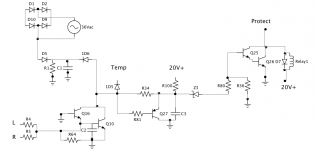
To your circuit, I think there are several mistakes: D1,D2,D3,D4 arranged incorrectly, gnd missing (that plus D5,R1,C1,1D6 is a quick turn-off circuit) / emitter of Q10 should be at gnd / 1D5 should be reversed / D7 should be reversed / what I am missing is a latching mechanism that retains the fault condition (=relay OFF) until you switch off mains power.
p.s. We're not in a hurry 🙂
I realized after I posted that d3,d4 are backwardsGood idea as destruction of one part often causes damage to others. The worst thing that has happened to me was a 1000W ISOTOP transistor dumping all the energy stored in a 150V 4F (Farad!). Looked and sounded really nice 🙂 After the smoke cleared, we could see that almost all IC's on the low voltage side had small holes in their cases. The interesting thing is that low and high voltage parts are completely isolated using optos and DC/DCs.
To your circuit, I think there are several mistakes: D1,D2,D3,D4 arranged incorrectly,
center-tap xformergnd missing
thanks, wondered about that(that plus D5,R1,C1,1D6 is a quick turn-off circuit)
I'll check for a ground but couldn't see it last time/ emitter of Q10 should be at gnd
I'll recheck them./ 1D5 should be reversed / D7 should be reversed
/ what I am missing is a latching mechanism that retains the fault condition (=relay OFF) until you switch off mains power.
p.s. We're not in a hurry 🙂
Absolutely not. 😀 thanks again for all your assistance. Btw, I asked Samson Audio for a schematic but no reply.
Hi,
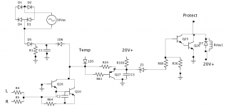
Q25 & 26 are the relay driver.
Q26 should be saturated when the relay is active, i.e. Ibq26*10 = Icq26 = Irelay
q25 must supply this current, when turned on by R80 going high.
R100 and C3 are the turn ON delay.
20V charges C3 through R100, voltage rises until Z3 starts to pass. Some current from R100 is bled off to pass through R36 and Q25 base. This slows down the rate of charge building up in C3.
Q27 is the fault detector.
When Q27 passes, it discharges C3 and the relay goes to OFF.
1D5 passes on a high temp condition to turn OFF.
D1,2,9,10 pass on AC pulses to keep C1 charged. when loss of AC occurs C1 discharges through R1 and 1D6 passes on loss of AC conditiion and relay goes to OFF.
L4 (&L5) pass speaker signal to Q16 Q10. This detects excessive voltage on C2
when Voltage on C2 is higher than trigger voltage Q16 or Q10 short out C3 and relay goes to OFF.
Does all this make any sense?
Which components went faulty?
BTW, every part of this circuit has at least one feature that I would not adopt.
In my view it is badly designed for the protection job it was intended for.
Thanks v. much Andrew.
D5 was shorted, 1D6 was opened and Q10 was destroyed. I was thinking of replacing all those plus Q16 and C2. Have you any suggestions on improving the design? What shortcomings do you see in it?
D5 was shorted, 1D6 was opened and Q10 was destroyed. I was thinking of replacing all those plus Q16 and C2. Have you any suggestions on improving the design? What shortcomings do you see in it?
the relay current is not well defined.
The diode slows done the relay release.
The base current of Q26 is not well defined.
R36 introduces an extra variable to the rate of charging of C3.
Temperature switch activation is OK.
The two transistor + C2 is not a good way to detect output offset.
C1 slows down response to loss of AC.
Find Self's article in this Forum and see how well it can be done.
in which sense?the relay current is not well defined.
If you mean D7, that is necessary to provide a path for inductive current after Q26 turn-off. This is equivalent to shorting the relay coil.The diode slows done the relay release.
Don't agree. I assume Z3 has a breakdown voltage close to 20V, so C3 charge is not disturbed while Z3 is not conducting. As soon as Z3 starts conducting, base current of Q25 develops rapidly (depending on component values: Q25/Q26 large hfe, R100 << R36) which terminates the startup procedure. After this, C3 charge behavior is irrelevant. I would omit R80 though.The base current of Q26 is not well defined. R36 introduces an extra variable to the rate of charging of C3.
C2/R64/R4/R5 act as a low pass filter for the audio signal, to prevent Q16 or Q10 from triggering from normal audio signal. Nothing against this in my opionion, except that I would add two zeners back to back to obtain a more precise trigger threshold.The two transistor + C2 is not a good way to detect output offset.
That is by intention, there must be some filtering to prevent triggering with the first missing half wave.C1 slows down response to loss of AC.
I think adding a Zener in series with D7 (anode to anode) is what Andrew had in mind, is that not right Andrew?
Hi Some,
you have read me right.
Read Self for a full explanation of why all those circuits need improved and how he suggests we achieve that.
you have read me right.
Read Self for a full explanation of why all those circuits need improved and how he suggests we achieve that.
Tatus,in which sense?
I have returned to this thread repeatedly over the last few days awaiting a final reverse engineered schematic.
I have seen it and now added my comments.
Do you think I would want to do that to deliberately mislead you, or is it possible I believe in what I have taken time to think through and present?
- Status
- Not open for further replies.
- Home
- Amplifiers
- Power Supplies
- Faulty supply problem


