Hi
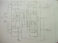
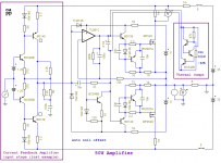
One thing about Hexfets, and other similar vertical fets, they are fast. The question is how much of that speed can you turn into usable BW? And how can you combat the inherent non-linear characteristics within? Simplicity is relative with these types of devices, that is if your goal is low distortion and good stability. It is certainly possible to ascertain these goals. Here is a quick example sketch I just made of a circuit similar to what I'm currently using for vertical fets. There will be some minor upgrades in the future.🙂
First thing to get right is stability. These devices may not show in simulation their unstable nature when inserted into an actual PCB as well as their destruction due to not having a protection Zener from gate to source. A great way to keep these devices stable is with a gate LP filter instead of just a gate stopper resistor as close to the device as possible. This allows you to increase the roll off slope and gain extra BW with less phase shift. The gate stopper alone creates a LP filter with the internal capacitances of the mosfet and can dampen the parasitic but capacitance value and Fc becomes somewhat dependent on the operating point of the fet. A decoupling capacitor at the drain as close to the device as possible is also a must. At MHz frequencies in the range of resonance for these devices, the inductance effects of the device pins can become significant.
In order to drive a vertical fet at a fast rate of change in conductance, it requires charge to increase the conductance as well as to turn the device off. A suitable driver stage should bias about 20-30mA. For a source follower configuration, a drive voltage of Vd + Vgs + delta Vgs is required. The pre-driver stage shown here uses a few mA of current and the driver stage is bootstrapped from the output. Since it is impossible to find two complementary vertical fets that match in both Gm and in gate charge, the two devices will require different amounts of charge and discharge to be moved into and out of each gate so two separate paths are used here. +/- 10V is supplied by the VAS. The error amplifier transistors as well as the next driver stage use small signal RF transistors. Cascode is used because RF devices are typically <20Vceo. Thermal compensation is done by allowing the error amp transistors (the ones with the star) to be in contact with the drain pin of the respective output device. A clamp prevents overcharge of the gates when the output devices are saturated.
It is important to keep PCB traces as short as possible for the RF paths within the EC loops. This will make the EC more effective. I think Hexfets make great power output stages. They are fast and very tough if you can fix the non-linear nature of the device. And I have also found the planer stripe type vertical fets to be able to take significant amounts of abuse.
One thing about Hexfets, and other similar vertical fets, they are fast. The question is how much of that speed can you turn into usable BW? And how can you combat the inherent non-linear characteristics within? Simplicity is relative with these types of devices, that is if your goal is low distortion and good stability. It is certainly possible to ascertain these goals. Here is a quick example sketch I just made of a circuit similar to what I'm currently using for vertical fets. There will be some minor upgrades in the future.🙂
First thing to get right is stability. These devices may not show in simulation their unstable nature when inserted into an actual PCB as well as their destruction due to not having a protection Zener from gate to source.
A great way to keep these devices stable is with a gate LP filter instead of just a gate stopper resistor as close to the device as possible. This allows you to increase the roll off slope and gain extra BW with less phase shift. The gate stopper alone creates a LP filter with the internal capacitances of the mosfet and can dampen the parasitic but capacitance value and Fc becomes somewhat dependent on the operating point of the fet. A decoupling capacitor at the drain as close to the device as possible is also a must. At MHz frequencies in the range of resonance for these devices, the inductance effects of the device pins can become significant. In order to drive a vertical fet at a fast rate of change in conductance, it requires charge to increase the conductance as well as to turn the device off. A suitable driver stage should bias about 20-30mA. For a source follower configuration, a drive voltage of Vd + Vgs + delta Vgs is required. The pre-driver stage shown here uses a few mA of current and the driver stage is bootstrapped from the output. Since it is impossible to find two complementary vertical fets that match in both Gm and in gate charge, the two devices will require different amounts of charge and discharge to be moved into and out of each gate so two separate paths are used here. +/- 10V is supplied by the VAS. The error amplifier transistors as well as the next driver stage use small signal RF transistors. Cascode is used because RF devices are typically <20Vceo. Thermal compensation is done by allowing the error amp transistors (the ones with the star) to be in contact with the drain pin of the respective output device. A clamp prevents overcharge of the gates when the output devices are saturated.
It is important to keep PCB traces as short as possible for the RF paths within the EC loops. This will make the EC more effective. I think Hexfets make great power output stages. They are fast and very tough if you can fix the non-linear nature of the device. And I have also found the planer stripe type vertical fets to be able to take significant amounts of abuse.
Attachments
Last edited:
Thanks, CBS.
Your sketch is already with error correction input. I am yet pace them, may be soon.
I know about gate ringing and sometimes spice models are just unfair.
This driver are two connected, not common gate as usual to minimize gate charge/discharge when operated at high speed. I am also using this in my qiasi driver.
Gate source voltages are highly damped with Rgs.
It draw 50mA at idle for low power and more than 100mA for high power, that is why I use floating supply.
I like to use IRF540 instead of IRFP240, because I feel something wrong with the model, and not the same as its real condition. I like to compare my real results with simulation for IRF540 and always small differences in compensator. And it act different in higher voltage, that not happened in simulator.
I never trying vertical fet.
Here I post IRFP result:
Attachments
Hi CBS, is that you mean with vertical mosfet is DMOS?, not VMOS? but planar stripe fet is still expensive.
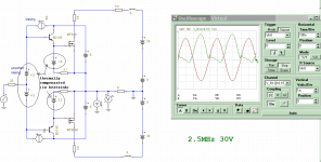
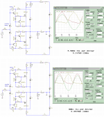
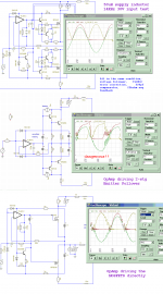
Simulation of its performance is finished. I am using 500uH supply inductors and 14KHz 30V input. Supply ringing very bad, and it ringing whole the circuits. This driver is very stable, not far from an emitter follower.
Simulation of its performance is finished. I am using 500uH supply inductors and 14KHz 30V input. Supply ringing very bad, and it ringing whole the circuits. This driver is very stable, not far from an emitter follower.
Attachments
Hello ontoaba
Would you mind telling me what software you're using. Looks quite good.
Regards
Mike
Would you mind telling me what software you're using. Looks quite good.
Regards
Mike
hello Mike,
It's Tina-TI 7, free version from texas instrument. You may download it at their website, or search it with google.
Regards
OA🙂
It's Tina-TI 7, free version from texas instrument. You may download it at their website, or search it with google.
Regards
OA🙂
Hi CBS, is that you mean with vertical mosfet is DMOS?, not VMOS? but planar stripe fet is still expensive.
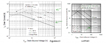
Vertical mosfets tend to have an exponential relationship between Vgs and Gm while lateral types tend to adhere to the Square law for Vgs vs Gm function. Planer stripe diffusion mosfets such as Fairchild's Q-fet line are like this in charactoristics, and like all verticals they are designed for switching. Also they are fairly cheap, at least in the US. For example. For DC operation this TO-220 device is capable of about 25W @ 150C. 😱 Cdg and Cds is a bit greater for the planer stripe types though.
The picture illustrates the major difference in die structure between planer stripe and multi-well devices such as IR's Hexfet.
Attachments

hello Mike,
It's Tina-TI 7, free version from texas instrument. You may download it at their website, or search it with google.
Regards
OA🙂
Thanks, OA.
Still using my ancient B2SPICE. Will try out TINA.
Mike
Free Ltspice from Linear.com is unlimited, Pspice compatable, used by Linear's own engineers, very much an engineer's version of Spice - no cute "gages" or "Oscilloscopes" but great convergence, speed, and funtionallity - "flat" UI means you do more with fewer, well concieved, powerful features - very active maintaince - bugs often fixed in near weekly releases - good support in the (members only) Yahoo users group
Mosfet speed is mostly packaging, wiring parasitic limited - except for polySi gate resistance limiting speed in some devices
if anyone Really wanted speed: http://www.ixysrf.com/products/hf.html
Mosfet speed is mostly packaging, wiring parasitic limited - except for polySi gate resistance limiting speed in some devices
if anyone Really wanted speed: http://www.ixysrf.com/products/hf.html
Last edited:
My experience of making a fast driver is that once I have one I then end up slugging it with capacitors to stop oscillation on the output !
I use the good old MJE340/350 in my VAS stage. Never let me down yet.
I use the good old MJE340/350 in my VAS stage. Never let me down yet.
My experience of making a fast driver is that once I have one I then end up slugging it with capacitors to stop oscillation on the output.
Is this oscillation your experiencing at the output caused by parasitics or from instability in the previous amplifier stages? Mosfet parasitic caused oscillations are very high in frequency and I have found that the Mosfet may ring at heavier loads and lower Vds. IOW, at the peak region of the waveform there may exist a small oscillation burst, well into the 10's of MHz. My experience with this specific problem is that a larger gate stopper will control it but at the expense of BW and phase shift, but a simple gate filter complemented with good PCB layout and keeping device pins short will dampen it proper.😎
Thanks, OA.
Still using my ancient B2SPICE. Will try out TINA.
Mike
OK🙂.
Hi, CBS.
I comparing their datasheets and planar stripe has better avalanche (rugged) and better SOA, very good for TO220. Much tougher than HEXFET. For 10mS this TO220 has IRFP260 strenght😱.
I am also attach a 50W PA schematic.
Attachments
Yes, I can crank out >100WRMS @ 8R with just 2 pair.😀 Here is a link to the circuit I made using planer stripe Q-fets. But power is not the whole story, it is important to have some sort of local EC driving them because the previous amplifier stages lack the BW required to really have a good effect on 'correcing' the non-linear nature of these devices.
Also Here is a paper by Bob that is relevant
Also Here is a paper by Bob that is relevant
Last edited:
My experience of making a fast driver is that once I have one I then end up slugging it with capacitors to stop oscillation on the output !
This one has 11nS lag, very safe from getting oscillated, when compared with normal drivers.
Hi,CBS, That Cordell output stages are looks similar with yours. In that paper, it reach very high linearity, isn't it also happened to your Q-fet? or is there something else happened?
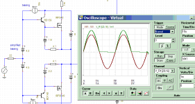
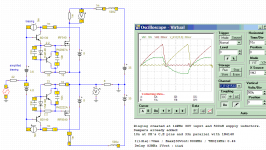
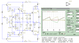
Here I post some comparison. Quick output stages are better than the slower.
Here I post some comparison. Quick output stages are better than the slower.
Attachments
Last edited:
Hi
I hope you understand the premise. It is all based on Dr Hawksford's error corection for Darlington transistors, long ago.
Here is a reference to the original publication. This basic stratagy has been adapted to vertical mosfets and does work pretty damn well. Honestly, I will probably never use a large power BJT as an output device ever again. However for lower power, medium power BJT OPS would be suitable and efficient.
I am leaving BJT output transistors 5 or 6 years ago. And now Q-fet has much tougher than other DMOS, I am also comparing this TO220 with sanken A1494 and its secondary breakdown makes it not even better than TO220 planar stipe for 10mS.
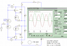
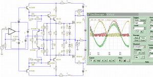
This is simulation result of R.R. Cordell output stage, error correction used is only decreasing THD by half, but it slow down the output stages more than twice. Similar with alison output stage that people trying to improve it in other thread.
This is simulation result of R.R. Cordell output stage, error correction used is only decreasing THD by half, but it slow down the output stages more than twice. Similar with alison output stage that people trying to improve it in other thread.
Attachments
Last edited:
- Status
- Not open for further replies.
- Home
- Amplifiers
- Solid State
- FAST and SIMPLE driver for HEXFETS (linear use).