Hi,
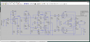
I have some difficulty with LTSpice simulation of HK Citation II. The only difference from the original is an output CFB transformer (real unit with real DCR of windings). Simulated amp oscillates even at low input signal level. Polarity of secondary connection (to GND / global feedback) is correct, reversing it causes huge spikes. Suppressor grid of 12BY7 pentode is connected to cathode in schematic, yet LTSpice models made as tetrodes with that connection already in place. 12BY7 models are by Ayumi (used), and another by Steve/Stepnie Bench (unused). Tried second, sim doesn't work either. All files in attachment.
Made similar simulations in the past, they were surprisingly close to real units when they were built and measured, even THD values.
I can't understand purpose of 4uF C7 (on original manufacturer's schematic), which is connected between grid and screen ("-" of that cap IMHO should go to the ground), but don't think its a bug in drawing.
Thanks in advance for any help.
Attachments
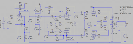
The local feedback from the top 12BY7 is going to the wrong side (both feedbacks are meeting at the same point!), it works if you bring the plate-to-grid feedback network comprising of R23 and C7 (in ltspice) to the junction of C5 and C3 (also in ltspice), i.e it's going to the correct grid!
Last edited:
Oh, to answer your question about C7, the negative end going to the cathode instead of ground is correct - it's the screen bypass capacitor, and the screen wants to be a constant voltage above the cathode at AC. It's not the end of the world if it is actually grounded instead, but it's "correct" place is indeed the cathode.

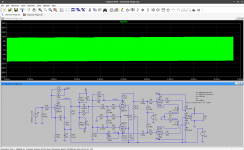
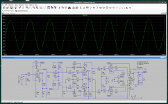
Bigwill thanks, actually there were 2 bugs in my LTSpice schematic. I corrected them and now it works. What is that strange shift of output signal symmetry, marked with red lines? Warm up of the amplifier?
PS. Steve/Stephie Bench 12BY7 LTSpice model (marked with "_sb" suffix) seem to be buggy.
PS. Steve/Stephie Bench 12BY7 LTSpice model (marked with "_sb" suffix) seem to be buggy.
Attachments
That shift you see is entirely normal and to be expected - it's a mathematical consequence of a non-infinite sine having a slight DC component - you are seeing the sine superexposed onto the exponential decay of said offset as it passes through an AC coupled amp.
There's nothing in the simulation to include the effects of warmup, so that's not it. What you're seeing is the effects of a large RC time constant. I'm guessing the coupling caps into the phase splitter or the 50 uF in the power supply for the input stage is to blame.
Note the time scale. We're looking at less than a second of simulation time.
These things are pretty common in simulations of circuits with long RC time constants. If I'm looking at steady-state behaviour of a circuit, I'll often run the simulation to, say, 5-10 seconds and only store the last few ms of data. Not storing the data speeds up the simulation. That's especially important if you want to look at low level distortion where the DC settling tends to throw off the THD calculation.
Tom
It sometimes helps somewhat to use the sum of a cosine of amplitude A and a fast step from -A to 0, instead of using a sine. The sum has to be zero during the DC operating point analysis, jump to the cosine's peak value just after t = 0 and then follow the cosine.
What is the formula to calculate K (coupling factor used by LTSpice) from Ls (leakage inductance)?
If I calculated it correctly, k = sqrt(1 - Ls/L) where Ls is the spreading inductance and L the total inductance measured on the same side of the transformer as the spreading inductance.
I tried my transformer model in this amplifier, but couldn't get a perfect match with the inductance values.
Also added a port-type input/output for the labels for the feedback to make the schematic more clear.
Put the 3 files from the zipfile in the same directory as Amp_Cit2.zip to give it a try.
Also added a port-type input/output for the labels for the feedback to make the schematic more clear.
Put the 3 files from the zipfile in the same directory as Amp_Cit2.zip to give it a try.
Attachments
I tried my transformer model in this amplifier, but couldn't get a perfect match with the inductance values.
Also added a port-type input/output for the labels for the feedback to make the schematic more clear.
Put the 3 files from the zipfile in the same directory as Amp_Cit2.zip to give it a try.
I would suggest to stay with mine transformer model, unless you have a real transformer with all parameters measured and recorded into SPICE model you would like to test in this very demanding circuit.
Both models are identical: coupled inductors with a K-factor. The only difference is that mine is hidden in a subcircuit.
If I do the math, 38.836 / 8.6 / 1.551 H doesn't match 30% UL and 12% CFB.
I calculated 336H, 32%UL, and 13.6% CFB. If I enter those values in my model, the inductors match yours.
The resistance of L1/L4 and L2/L3 are not equal in your model. Is that intentional?
If I do the math, 38.836 / 8.6 / 1.551 H doesn't match 30% UL and 12% CFB.
I calculated 336H, 32%UL, and 13.6% CFB. If I enter those values in my model, the inductors match yours.
The resistance of L1/L4 and L2/L3 are not equal in your model. Is that intentional?
I checked again my spreadsheet, sorry, send you wrong data, correct numbers are 32% UL and 12% CFB. Since inductance is not constant, I took a prototype transformer I designed and made some time ago. number of turns, core/winding geometry, average permeability 10000 and air gap 0.1mm. Leakage inductance was 4.39mH, its quite small and won't have much of effect. Parasitic capacitance will play major role, yet its quite difficult to program into SPICE model with a transformer with so many winding sections. And I see no reason to do so in this particular case. Also, I can't explain benefits of turning transformer into sub-circuit unless you want to examine behavior of very different units.
The resistance is not equal because outer layers have longer mean turn length, and therefore, higher DC resistance.
I'm building Citation II on a prototype board right now, and before that, wished to model its behavior, incl. THD analysis. Probably I will decrease its GNFB to match sensitivity about to 0.25V instead of 1.5V. CFB will reduce distortions of the output stage which contributes most of bad stuff.
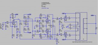
Original schematics have some oddity (if its not a print bug). Please note grid of the upper U1 KT88 is being connected not to the anode of the phase splitter U7, but to the voltage divider / junction of R11/R13. I checked 2 different release/printouts of Citation II schematics, they all have this connection in this way. In order to balance output signal I made adjustment of 5K potentiometer to ratio 0.95. In turn, this have created considerable asymmetry of anode voltage for 2 tubes of the phase splitter (267V and 320V respectively).
Is this a deliberate way (made by designers of this amp) to increase 2nd order harmonics over 3rd?
Complete set of files attached as always.
Is this a deliberate way (made by designers of this amp) to increase 2nd order harmonics over 3rd?
Complete set of files attached as always.
Attachments
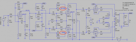
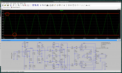
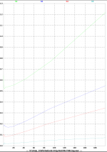
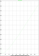
I made a sym of THD analysis, and my assumption of artificial asymmetry in phase splitter was correct. Look at the files attached, voltages at phase splitter anodes, and THD harmonics (1.5V input, 60W output). 2nd order harmonic becomes predominant thanks to asymmetry.
Attachments
- Home
- Amplifiers
- Tubes / Valves
- Failed LTSpice Simulation of HK Citation II