Hi,
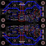
Some time ago I started playing with Jung/Didden superreg PCB design with the attempt to make it smaller. But soon I realized that it is hard to change the board's footprint… The length is determined by the size of the pass transistor heatsink plus the caps before and after that transistor and then the connectors/mounting holes. The width is also hard to minimize because of 4 way output connector and two mounting holes. So I ended up with the PCB which by ~90% follows the design from Jan Didden. I used smaller footprint electrolytic caps (inspired by the size of Panasonic FC caps). I also added labels to the connectors (which are really lacking on the original PCBs IMHO) and a short note for output voltage setting. The board view is attached. Component numbers are the same as on the original schematic of recently published V2.3 PCB from Jan Didden. My obsession with symmetry lead to even more symmetric layout and I hope I did not screw up by ''symmetrizing”.
If anyone sees any obvious errors with the layout please comment. I would be glad to fix it before going for production.
OlegSh
PS: If it does not interfere with the Superreg offer from the diyaudio store and there are no other concerns I can post Eagle files if there is interest.
Disclaimer: the boards are for my own use. No commercial use is intended.
Attachments
Actually you *could* make them smaller but you would have to leave the (sort of) diyaudio standard of 10mm hole grid.
All in all, I believe the PCB is pretty well optimized, recognizing that ANY design can be improved if you throw enough effort at it, but you get to the area of diminishing returns.
The SMD caps across the connector points are a nice touch.
No problem for personal use, but I specifically turned the PCB design over to diyaudio to help them with the forum costs. I'm not getting anything out of it, and I would hope you wouldn't get into competition with them.
So, your 'failed attempt' didn't really fail at all!
Jan
Thanks a lot for your comments, Jan!
I will not publish the design files then. I did not intend to compete with diyaudio...
But if you or diyaudio admin are interested I can forward the files to you.
OlegSh
I will not publish the design files then. I did not intend to compete with diyaudio...
But if you or diyaudio admin are interested I can forward the files to you.
OlegSh
Sure🙂 I'll report back if it all works as intended...
That's boring. Report back if it does NOT work as intended 😀
Jan
If you can't make it smaller, make it bigger!
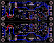
I have added a bulk rectifier and CRC filter before the regs (attached). Now it only requires dual secondary transformer to get going.
I just have a small concern about the proximity of power resistor to the filter cap. If I choose the resistor value around 1~2 Ohm I think I'll be fine but higher values would heat the nearest cap to much. Max current I intend to draw from each leg is around 500 mA.
So could someone tell me where is a practical range of values for the CRC filter resistance for around 500 mA output? Would a resistor in the range of 1~2 Ohm be fine there or it is to small to have a noticeable effect?
Regards,
Oleg
Attachments
You could use 0.22R if you want. But it depends on the cap (and inductor) values. Lesser than that may introduce peaking (if an inductor is used, see below). Higher than that is not necessary because the JSR has such a high PSRR at low frequencies.
If you use CRC instead of C, why not use CLRC? I use 47uH + 2.2uH shielded inductors as the L. The lower value inductor has a much higher resonant frequency and this is what is needed. An inductor here helps reduce RF substantially! Active devices are not very good dealing with RF, so let the LC filters get rid of the RF first before the regulator. I got much better result doing this.
If you use CRC instead of C, why not use CLRC? I use 47uH + 2.2uH shielded inductors as the L. The lower value inductor has a much higher resonant frequency and this is what is needed. An inductor here helps reduce RF substantially! Active devices are not very good dealing with RF, so let the LC filters get rid of the RF first before the regulator. I got much better result doing this.
Thanks for the hints HiFiNutNut!
Is it fine to use the 47uH inductor with the DCR around 0.22~0.5 Ohm eliminating the need for a series resistor?
Unfortunately I do not fully understand the use of two inductors. Could you please elaborate?
Regards,
Oleg
Is it fine to use the 47uH inductor with the DCR around 0.22~0.5 Ohm eliminating the need for a series resistor?
Unfortunately I do not fully understand the use of two inductors. Could you please elaborate?
Regards,
Oleg
Finally understood the use of two inductors in series. The effect should be similar to paralleling different value caps for ICs power lines decoupling - addressing different frequencies due to different self-resonance frequencies.
Now I have another question. I'm designing my own PCBs for the B1 buffer to be used with the superregs. Is it wise to extend the sense connection to the actual load point on the buffer PCB? Or it is better to connect the sense wires together with the supply wires at the buffer's power connector?
Regards,
Oleg
If you can get the sense lines as close to the actual load as possible. They called 'sense' for a purpose 🙂
jan
jan
Thanks Jan!
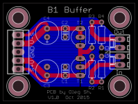
Attached is a current state of my B1 PCB design. I've connected the pos/neg sense lines to the small electrolytic caps on the supply lines on the buffer PCB assuming that the voltage change on the small (film or ceramic) decoupling caps is too fast to be traced by the regulator. Is it the right assumption or I can extend the sense lines all the way to the transistors?
Regards,
Oleg
Attachments
Thanks Jan!
Attached is a current state of my B1 PCB design. I've connected the pos/neg sense lines to the small electrolytic caps on the supply lines on the buffer PCB assuming that the voltage change on the small (film or ceramic) decoupling caps is too fast to be traced by the regulator. Is it the right assumption or I can extend the sense lines all the way to the transistors?
Regards,
Oleg
Well in principle you'd want them where you want the cleanest supply, and that's at the transistors. But in this practical case it won't make any difference.
What is the purpose of R4 ?
Mona
It is a mega Ohm resistor from output to ground and if I understand it right it is there to provide the output return to ground if load is disconnected.
Thanks a lot Jan!
I understand that with such a short distances it is not going to make much of a difference, but I'll reconnect the sense to the transistors.
I understand that with such a short distances it is not going to make much of a difference, but I'll reconnect the sense to the transistors.
Thanks a lot Jan!
I understand that with such a short distances it is not going to make much of a difference, but I'll reconnect the sense to the transistors.
You need to think: where do I want the cleanest supply? That's the point you want to connect the sense.
Is it important to have clean supply at the cap? Not primarily - the cap is there to help get the cleanest supply at the load.
In this case with very low R and L between that cap and the load to generate any potential difference across the short trace, you won't see a difference.
Jan
I understand the reasoning behind the sense connection. My only (most probably naive) concern was/is thas the capacitors act as the load to the regulator as well and while being in between the regulator and the actual load point they can interfere with "delivery" of clean potential to the actual load due to finite time constant of the sense feedback. On the other hand too fast transients would not be seen by the regulator due connection line inductance. Thus I assumed that the local voltage reference on the buffer PCB can be the electrolytic cap assuming that If I would keep its potential constant it will ensure clean power at the loading point down the line.
Otherwise the need for the capacitors on the buffer PCB is questinable...
Otherwise the need for the capacitors on the buffer PCB is questinable...
Thanks again Jan! You made me think.
Now I have an impression that the only benefit of having extra connection for the sense lines on my buffer PCB is to compensate for the contact impedance of the power line connectors.
Now I wonder what value electrolytic caps are suitable on the buffer board if it is fed by the supperregs from a distance of around 5 cm? Would something around 47uF be OK? As I've seen in the original superreg thread you mentioned that large capacitance is not needed on the load side in combination with superregs but what is needed?
Thanks,
Oleg
- Status
- Not open for further replies.
- Home
- Amplifiers
- Power Supplies
- Failed attempt of Jung/Didden superreg PCB redesign