already done with laterals
however - their Xconductance is lower , comparing to verticals;
less OLG , so less feedback , different THD spectra
'cause I didn't compared it with original , can't say what's difference in sound
however - their Xconductance is lower , comparing to verticals;
less OLG , so less feedback , different THD spectra
'cause I didn't compared it with original , can't say what's difference in sound
could you post any schema or bias resistor mod for it?
Use the Ohm's Law - if your JFETs work at Id of, say, 5mA and you need 2V of Vgs to bias the LATFETs at about 1A you'll need JFETs' drain resistors to be around 400 R (use 1k multi-turn pots and omit LATFETs' Rs, NTC and the rest of parts HEXFETs need for thermal compensation). Since LATFETs have lower parasitic capacitance meaning that they need less gate drive than HEXFETs it would be beneficial to use GR grade JFETs (lower ID) since that way their drain resistors will be higher and the OLG won't drop (maybe a little since the GR grade parts have lower gm).
I got good results by using the BJTs in the input stage at the Ic of about 3mA. I proposed that solution few years ago and can't search for those posts now but you can see it in Lazy Cat's thread about VSSA - that's F5 gone BJT with LATFET Source Follower output stage added.
Last edited:

Not clear what do you mean - can't make F5 with j74 only, what extra stage?...to avoid one extra stage, going only with J74GR the gain will be too low?
Feedback net usually employs 2 resistors. Reducing one of them will increase the gain and distortion (and the Id in the input stage too). Again, it's not clear what you really mean ?I could reduce the feedback resistor, but then distortion will be higher?
What ? Few ideas are already mentioned and each will sound different...how will it sound?
It's a transconductance amp, like BA-3. Its gain is determined as G=1A/V and the voltage on the speaker will largely depend on its impedance, so voltage gain cannot be declared as high or low since it depends on the speaker.found one schema of a sort of it but with even less gain and no feedback:
Absence of feedback makes it what it is. Insert a feedback loop and you'll get pretty standard amp.
Please, try to be more articulate and specific - you'll get more help that way
Sorry I was too fast in writing last time...
I would like to keep the original F5 2 stage design. Avoid to add a transistor stage to drive the 2sj162 2sk1058
Will the OLG be too low with laterals?
I would like to keep the original F5 2 stage design. Avoid to add a transistor stage to drive the 2sj162 2sk1058
Will the OLG be too low with laterals?
Avoid to add a transistor stage to drive the 2sj162 2sk1058
indra's suggestion to use the LSK pre to drive the laterals
http://www.diyaudio.com/forums/pass-labs/244106-lsk-pre-baf-2013-a-3.html (post#76)
Nobody mentioned additional stage to drive LATFETs. Just put them in circuit instead of HEXFETs and do as written in post #4....I would like to keep the original F5 2 stage design. Avoid to add a transistor stage to drive the 2sj162 2sk1058
No. Maybe lower (depending on input stage parts choice) but not too low.Will the OLG be too low with laterals?
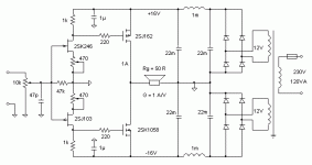
As it usually happens, looking for something else, today I found my F5 version with Lateral MOSFETs that I mentioned in post #4.
Laterals here need no source resistors and no thermal compensation.
3.5mA runs through the each of the input BJTs - BC550C/560C work here great too (matching is beneficial but not mandatory).
Biasing procedure is the same as for the standard version - the only thing different is that you can bias LATFETs somewhat lower (1A is OK) since the absence of source resistors and the specific curvature of MOSFETs' transfer characteristic enables much later (in terms of load current) switching to AB class regime.
Oh, and 4.7mF means 4700uF.
Attachments
Nobody mentioned additional stage to drive LATFETs. Just put them in circuit instead of HEXFETs and do as written in post #4.
Being mindful that the pinouts are different from the vertical MOSFETs.
Being mindful that the pinouts are different from the vertical MOSFETs.
It's a basic premise - to check the pinout of the component before it's built in the circuit.
Those who need an extra warning about that should wait some more before building anything...
Has someone tried to remove the big feedback caps by setting input BJT bias at base instead of emitter?
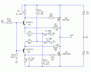
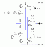
See example of input stage below.
Fab
See example of input stage below.
Fab
Attachments
Last edited:
Hi fab,
that won't work very good (power rail connected to BJT's base) unless you break each R67/R66 into two 10k resistors and connect the big cap (say 220uF) from their center point to ground. Stiff power rails are a must and a big input cap too (I think that 22uF input cap does a lot more damage than the feedback loop caps). You might want to rework that scheme with some diodes around bases in order to polarize input BJTs but input cap would still be needed.
If you want to lose feedback and input caps much better idea would be the one that Hiraga used in hs 20W cl. A amp (see attachment). But that one introduces one more pair of BJTs at the input as an emitter follower stage. I tried that one too but the sch. from post #10 still sounds better to me.
Regards!
Attachments
Hi fab,
that won't work very good (power rail connected to BJT's base) unless you break each R67/R66 into two 10k resistors and connect the big cap (say 220uF) from their center point to ground. Stiff power rails are a must and a big input cap too (I think that 22uF input cap does a lot more damage than the feedback loop caps). You might want to rework that scheme with some diodes around bases in order to polarize input BJTs but input cap would still be needed.
If you want to lose feedback and input caps much better idea would be the one that Hiraga used in hs 20W cl. A amp (see attachment). But that one introduces one more pair of BJTs at the input as an emitter follower stage. I tried that one too but the sch. from post #10 still sounds better to me.
Regards!
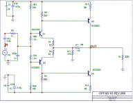
Hi Juma
Nice adaptation of the Hiraga input stage!
I am already aware of the Hiraga design. I have built 2 version and also the NX amp from Bonsai. Like you I prefer to limit the number of stages.
Thanks for the idea to filter input from rail (most important for a power amp) 🙂. R66/R67 could also be replaced by simple current diodes too. There should not be significant DC at input since it is at middle point of both supplies. The polarization is done with the, 2 resistors (R69/70) at base of BJT so no problem there...
I prefer the input cap anyway to protect the amp -then the speakers- from source or preamp possible DC ( failures) presence. So For that reason I think this circuit eliminates 2 feedback caps ( in reality 4 because of the bypass with 10uf too) and does not add an input cap....- at least this is my point of view.
Thanks
Fab
Last edited:
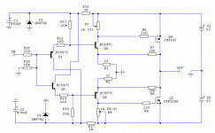
Hi Indra1,
it works theoretically but it will inject all the ripple from the power rails into the input BJTs' emitters (which are very low Z, and they are inside the feedback loop) and you'll have enormous hum at the output.
So if you want to pursue that idea you'll have to come up with perfectly clean power rails.
One possibility is to break your R9/R10 into two smaller resistor each an put the very big cap from their center point to GND but that brings us to worse solution than the one we started with...
Hi Juma, thanks for the comment. Seems that split R9/R10 with big cap is a partial solution at best. A shunt voltage regulator is probably a minimum acceptable solution. Or perhaps a good SMPS supply would be good enough. Will have to try.
Shunt reg for the front end won't work here because you can not disrupt the Vgs circuit of the MOSFETs.
It might be a better idea to use two CCSs (38-40mA) instead of R9/R10 since CCS has a large dynamic impedance and will dramatically improve PSRR.
Each CCS will dissipate almost 1W so LM317 used as a CCS comes to my mind - see Walt Jung's article about them.
Of course, a cap multipliers on the power rails will be beneficial.
- Status
- Not open for further replies.
- Home
- Amplifiers
- Pass Labs
- F5 with 2sj162 2sk1058 ?