..the top three legged thingies are 2 diodes and 2 transistors each side ...look closely at refs😀
Diodes
Thanks CeeVee,
I see it - I should have looked closer - I thought he was going for 4 pairs of outputs. The number of source resistors should have clued me in also.
Thanks,
Steve
Thanks CeeVee,
I see it - I should have looked closer - I thought he was going for 4 pairs of outputs. The number of source resistors should have clued me in also.
Thanks,
Steve
I think I'll trim off the waste board on each size. Should make manufacture a little cheaper. Even with the thickness of the tracks as they are I think I might go for 2oz board. Do you think 1.6mm board is thick enough or shall I go for 2mm?
2 mm would be nice , why not v3 , this one is not above the current f5 c boards currently available ...
Why not just reduce Rs,While the use of the more troublesome practice of parallel diode? Whether parallel diode will be more beneficial?
If you keep the diodes attached to the main heatsink, then I suggest you move them to between the FETs.
That lets you cut off the excess PCB to the left.
It also allows you to move the right hand pair of FETs closer to the middle of the PCB. This gets the 4 FETs on an equal spacing for more consistent Tc.
This could save 40 to 50mm of PCB length.
I think the diodes should be off the main heatsink.
That lets you cut off the excess PCB to the left.
It also allows you to move the right hand pair of FETs closer to the middle of the PCB. This gets the 4 FETs on an equal spacing for more consistent Tc.
This could save 40 to 50mm of PCB length.
I think the diodes should be off the main heatsink.
OK,
I've re-laid the board for F5 v3.
If you want to build an v2 just don't populate a pair of Power FETs per rail.
If you don't want to use the MUR3020's and know what your doing in regards to the Source Resistors; be my guest.
Cascaded 2SC4793 and 2SA1837 provided for as per v3 schematic.
They should also be used for a v2 to avoid operating the JFET's out of spec.
Comments and critisicms as always, appreciated
Andy
An externally hosted image should be here but it was not working when we last tested it.
Comments and critisicms as always, appreciated
Great!
If you could double (parallel) the input Fets one could add even more output pairs. Maybe a complementary B2 output board...
Hmm. It's getting a bit tight in the middle there.
It's worth it.
What's a B2 output board?
ooops I meant complementary BA-2 output board
Attachments
man...my boards evolved into something really nice.😉
yes my board did to.😀😀😀😀😀
And gues why I stand back
UKtoecutter work will make you free.
Do you mean paralleling up Q1 & Q2?
Yes!
And Mono Block is a very good idea also
Someone else can do the monoblock. My brain is fried!
JBL, I got you your two additional JFETs on board. I guess that could just be optional if somebody didn't want them.
I'm off to work away for a few days so I won't be able to edit board layouts sgain until Friday, but I'll keep an eye on the thread.
Best Regards
JBL, I got you your two additional JFETs on board. I guess that could just be optional if somebody didn't want them.
I'm off to work away for a few days so I won't be able to edit board layouts sgain until Friday, but I'll keep an eye on the thread.
Best Regards
An externally hosted image should be here but it was not working when we last tested it.
CeeVee,
Thank you. You are the inspiration for the layout. It's your layout with a few tweaks.
Andy
Thank you. You are the inspiration for the layout. It's your layout with a few tweaks.
Andy
JBL, I got you your two additional JFETs on board. I guess that could just be optional if somebody didn't want them.
Thank you for the work. To do it best the input jfets need to be thermally coupled. So the all need to sit together somehow. Looks difficult with the current layout. Hmmm as said I have no idea about pcb design.
CeeVee,
Thank you. You are the inspiration for the layout. It's your layout with a few tweaks.
Andy
It's great to work cooperatively like this....glad to give some back.😀
Your work on the PCB was fantastic....
Last edited:
Thank you for the work. To do it best the input jfets need to be thermally coupled. So the all need to sit together somehow. Looks difficult with the current layout. Hmmm as said I have no idea about pcb design.
JBL,
Please correct me if I'm wrong but I would have thought that as long as Q1 and Q2 are thermally coupled then that should be enough as the other pair are in parallel.
Can somebody explain to what the advantage of paralleling these devices is?
Will there not be an effect on the input impedance?
Andy
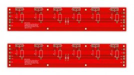
OK,
I've re-laid the board for F5 v3.
If you want to build an v2 just don't populate a pair of Power FETs per rail.
If you don't want to use the MUR3020's and know what your doing in regards to the Source Resistors; be my guest.
Cascaded 2SC4793 and 2SA1837 provided for as per v3 schematic.
They should also be used for a v2 to avoid operating the JFET's out of spec.
Comments and critisicms as always, appreciated
Andy
An externally hosted image should be here but it was not working when we last tested it.
Someone else can do the monoblock. My brain is fried!
JBL, I got you your two additional JFETs on board. I guess that could just be optional if somebody didn't want them.
I'm off to work away for a few days so I won't be able to edit board layouts sgain until Friday, but I'll keep an eye on the thread.
Best Regards
An externally hosted image should be here but it was not working when we last tested it.
Fantastic V3 🙂 ..........
- Status
- Not open for further replies.
- Home
- Amplifiers
- Pass Labs
- F5 Turbo Circuit Boards