Got it.
In order to make the PCB mount solder cups fit, I drilled out the boards and spoiled two vias. Once PCB mount solder cups were mounted the resistor ladder began to work properly.
Yiikes.
In order to make the PCB mount solder cups fit, I drilled out the boards and spoiled two vias. Once PCB mount solder cups were mounted the resistor ladder began to work properly.
Yiikes.
Just finished f5 v2, 36V rails, cascode 345mA bias.
WOW 🙂
Thank you Nelson Pass, I'd never get to enjoy music like this without your donated skills.
It's an amazing amp!
Thanks to 6L6 for the excellent build guide. I couldn't have completed my amp without it 😃
WOW 🙂
Thank you Nelson Pass, I'd never get to enjoy music like this without your donated skills.
It's an amazing amp!
Thanks to 6L6 for the excellent build guide. I couldn't have completed my amp without it 😃
Capacitors C1 and C2 are hung across the voltage rails close to the cascode BJT for front end voltage support. The schematic doesn't show a C1x or C2x. If you have these positions on your PC board then you could just stuff more capacitance, could hurt.
I'm quite a bit confused. If i swap V+ with V- and swap all P-ch mosfets/jfets with N-ch mosfets/jfets, all would work fine, right? I'm not using the source diodes (F5t v1).
Second question is, if people in the build guide say P1/P2 have to be close to 0 Ohms during first powerup, that means 0 Ohms between rail and jfet drain, right?
Second question is, if people in the build guide say P1/P2 have to be close to 0 Ohms during first powerup, that means 0 Ohms between rail and jfet drain, right?
Last edited:
Capacitors C1 and C2 are hung across the voltage rails close to the cascode BJT for front end voltage support. The schematic doesn't show a C1x or C2x. If you have these positions on your PC board then you could just stuff more capacitance, could hurt.
C1x and C2x are on the output boards.
C1x and C2x are on the output boards.
Interesting, I haven't seen the pcbs for front end and output seperate. My boards are one board per channel with the "front end" in the middle of the board, that's why I have no C1x and C2x. Follow your traces and see where they connect. Still if they are caps across the v rails then more is better.
Yay, my first channel runs 🙂
Not quite there yet to listen to music, but biasing is a lot of fun already. Building from scratch was fun, too.
Hopefully I'll be able to listen to it tomorrow.
Not quite there yet to listen to music, but biasing is a lot of fun already. Building from scratch was fun, too.
Hopefully I'll be able to listen to it tomorrow.
I've biased up to .7A, had DC offset going around +/- 2mV. So everything looks fine.
With 2 output-pairs, I can assume I draw 2.8A from the PSU, right? So 1.4A per rectifier, why does it get like 80-100C (case) then? 🙁 I'm using the gsib2560 ones. Checked everything, nothing else gets unexpectedly hot. Datasheet says T(JA) 22C/W, at 20C room temp that would mean it eats 3-4W. Why?
If it's supposed to be that way, are there special heat sinks available for these packages? I don't want anything running that hot inside the amp.
5am, time to sleep. Been a good day 🙂
The diode Vf varies with passing current.
The higher the diode current the higher the Vf.
At very low current say <1mA the Vf can be as low as <0.5Vf at room temperature.
Dissipation is 0.001A*0.5V = 0.5mW
At "normal" currents around 500mA to 2A expect the Vf to rise to 0.7Vf at room temperature, if you can keep them that cool. As the internal heat raises the diode junction temperature the Vf will drop a little, typically to 0.65Vf
Here we are dissipating ~1A*0.7V ~0.7W per diode if ON/passing all the time.
0.7W from a bare To220 diode will feel quite hot to the "finger" test.
At "high" current say 80% of rating (8A through a 10A diode) expect the Vf to rise to 2Vf at room temperature. The heat load is enormous and cooling will be required to prevent Tj going into "no go" range. The high Tj may bring the Vdrop down a bit, maybe 1.7Vf
The power dissipated is 8A*1.7V = 13.6W
That's why the cooling is required.
Often the diodes are operating on duty cycles <50%. That reduces dissipation to <6.8W
Last edited:
Would C1x and C2x be appropriate on the second board in a daisy chain?
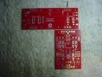
I too have the same question as BigE as to why C1x is there on the output board. Since these boards are new and most members are perhaps unfamiliar with them I have attached a pic. Checking continuity on the boards I can tell that C1x is between the power supply and G so it is similarly situated as on the FE board. The schematic only shows C1.
Since these are separate output boards is there need for adding more decoupling caps?
Perhaps it depends on whether one makes the V and G connections from the FE board to the output board or directly from the PSU board to the output board. If the latter then C1x should be populated is what I think to serve as decoupling.
Would appreciate if the more experienced would chime in.
Nash
Attachments
I too have the same question as BigE as to why C1x is there on the output board. Since these boards are new and most members are perhaps unfamiliar with them I have attached a pic. Checking continuity on the boards I can tell that C1x is between the power supply and G so it is similarly situated as on the FE board. The schematic only shows C1.
Since these are separate output boards is there need for adding more decoupling caps?
Perhaps it depends on whether one makes the V and G connections from the FE board to the output board or directly from the PSU board to the output board. If the latter then C1x should be populated is what I think to serve as decoupling.
Would appreciate if the more experienced would chime in.
Nash
I believe those are there for further decoupling of the rail supply voltage, if you need it. I guess the longer the wires are the more you may need that. But is optional.
Rush
Hi nebiki,
The transformers I originally used in the SA/1 vibrated so I potted them in 3M thermal potting compound. I know one builder who pots his transformers in high temp wax. No more mechanical hum.
Good Luck.
John
Do you have a link to the compound please ?
Do you have a link to the compound please ?
google came up with this: Invalid Request
too expensive, and the hum on my transformers isn't that bad. Placed them on top of some rubber and the vibrations are gone. Still a little humming noticable, but only when near the source.
The only problem I have right now is probably the source (using odac+o2). I get some white noise and weird noises when I move the mouse. Very annoying 🙁 Will check out some threads about the odac later.
I am quite confused again. Maybe someone can help me out here.
As I've said, I'm using an o2+odac combo with the F5. If i take the signal and its reference from the o2 directly into the input and audio ground, wouldn't that actually short both the o2's ground (which probably is USB ground, which probably is my computer's ground?) and my main audio ground?
Might that be the reason for the weird noise I'm experiencing? It gets enormously loud when I power off the o2. Any ideas? Sorry for weird questions.
And by the way, thanks Andrew 🙂 I think the "per diode" reference was the key. Checked with the datasheet of the rectifier which states that dissipation is ~1.5xI at below 2 amps. So if the temperature I feel is more 80 than 100 then all makes sense.
I believe those are there for further decoupling of the rail supply voltage, if you need it. I guess the longer the wires are the more you may need that. But is optional.
Rush
I guess, but what values do you use here? 10uF is awfully small, if it is supposed to deliver power for transients.
I don't see the one I used, will have to search my boxes of supplies for the last container but try -
3M 2135 Scotchcast Potting Compound
- Home
- Amplifiers
- Pass Labs
- F5 Turbo Builders Thread