I've been modeling the Pass F4 schematic.
Capacitors C3/C4 are coupled to Q1/Q2 through R24/R25, creating a voltage divider with R5/R22. It's also coupled to Q3-Q8 through R6/R7.
In other words, the AC output waveform goes through C3/C4 and directly modifies the bias of Q1/Q2 (which appears to be positive feedback), and also modifies the bias of Q3-Q8 through R6/R7 (which then fights the TL431's voltage).
Lowering or dropping R24/25 increases the amount of AC coupling. The overall gain increases slightly, but distortion also drops significantly. Removing C3/C4 decreases the gain slightly, but distortion increases again.
I don't quite understand the dynamics of C3/C4. Anyone care to explain? How is the value of R24/25 determined?
Attachments
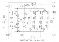
C3 and C4 bootstrap the rails voltages for the input JFETs
so that they will swing rail-to-rail while operating at less
than their voltage ratings.
You can eliminate all of that if you like, in fact the first
version published does not have this, but at maximum
swing the rated voltages of the input JFETs will be
exceeded. I have not seen a failure due to this, so feel
free to try it.
😎
- Status
- Not open for further replies.