Hi All!
I'm looking at trying to cobble together an F2J JIG that I can test UnitedSIC JFETS with. I'm not looking for the magical "Triode" like behaviour or any special tones. Just an amplifier of around 5 Watts with a relatively low distortion figure and can drive 88dbw/M speakers 6 OHM. (Paradigm Signature Reference S2) I spoke with Mr. Pass (Papa Pass) and he stated I can just plug them in and tinker and warned me about using depletion mode JFETS (which I have studied in class A self biasing modes) in the f2J, however he chose a rare variety of enhanced mode JFET. I asked my professor about these and he said they don't exist and told me to start designing with common parts! So, I looked into it further and actually they are mostly normally off devices (the common JFET needs a few volts negative to turn it on!) well... yes.. hes correct in that ALL of our tests and labs we are using small signal JFETS which are only depletion mode devices and enhancement mode devices are usually strictly Mosfets and further I learned today that they are now discrete cascode MOS/JFET design. (UJ4C075060K3S) which is actually a JFET/MOSFET in the same package. 🤔
My main idea for this year end project was to demonstrate a small 5w Amp using PAPA F2J to my class but instead of trying to find or buy rare R100 Semisouth devices I wanted to use something common like depletion mode devices from UnitedSiC, biased in CLASS A with liquid cooling; more specifically these SiC depletion devices I found and are easily available to me: UJ3N065080K3S or UJ3N120070K3S
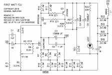
Using his production ready circuit and trying to "plug in" these devices will not work as the original F2J is using rare enhanced mode JFETS with positive bias on the gate, so...
My question what is the most elegant way to develop negative bias to the gate using a simple bench power supply? Obviously, Opening R4 and directing it to a negative voltage regulator source came to mind? Is there anything else I need to change in the F2J layout so that I can save some time and headaches with my project? I am seeking to demonstrate a low noise and low THD CLASS A amplifier with a liquid cooling system.
I hope to learn and build with modern Silicon Carbide or GaN devices so please go easy on me!
Thank you so much.
Jeff
I'm looking at trying to cobble together an F2J JIG that I can test UnitedSIC JFETS with. I'm not looking for the magical "Triode" like behaviour or any special tones. Just an amplifier of around 5 Watts with a relatively low distortion figure and can drive 88dbw/M speakers 6 OHM. (Paradigm Signature Reference S2) I spoke with Mr. Pass (Papa Pass) and he stated I can just plug them in and tinker and warned me about using depletion mode JFETS (which I have studied in class A self biasing modes) in the f2J, however he chose a rare variety of enhanced mode JFET. I asked my professor about these and he said they don't exist and told me to start designing with common parts! So, I looked into it further and actually they are mostly normally off devices (the common JFET needs a few volts negative to turn it on!) well... yes.. hes correct in that ALL of our tests and labs we are using small signal JFETS which are only depletion mode devices and enhancement mode devices are usually strictly Mosfets and further I learned today that they are now discrete cascode MOS/JFET design. (UJ4C075060K3S) which is actually a JFET/MOSFET in the same package. 🤔
My main idea for this year end project was to demonstrate a small 5w Amp using PAPA F2J to my class but instead of trying to find or buy rare R100 Semisouth devices I wanted to use something common like depletion mode devices from UnitedSiC, biased in CLASS A with liquid cooling; more specifically these SiC depletion devices I found and are easily available to me: UJ3N065080K3S or UJ3N120070K3S
Using his production ready circuit and trying to "plug in" these devices will not work as the original F2J is using rare enhanced mode JFETS with positive bias on the gate, so...
My question what is the most elegant way to develop negative bias to the gate using a simple bench power supply? Obviously, Opening R4 and directing it to a negative voltage regulator source came to mind? Is there anything else I need to change in the F2J layout so that I can save some time and headaches with my project? I am seeking to demonstrate a low noise and low THD CLASS A amplifier with a liquid cooling system.
I hope to learn and build with modern Silicon Carbide or GaN devices so please go easy on me!
Thank you so much.
Jeff
Attachments
Last edited:
just use separate (no need for more than 50mA capacity) rail for biasing duty
and then there is issue of modern depletion parts having abundant xconductance, so you'll need either significant source degeneration, or negative feedback, or both - to keep gain of amp in normal range
and then there is issue of modern depletion parts having abundant xconductance, so you'll need either significant source degeneration, or negative feedback, or both - to keep gain of amp in normal range

The current crop of depletion mode power fets seem to want something around -10 volts of Gate bias. Not a problem with common drain mode, but more complicated with common source mode.
Would it be possible to setup the depl FET in common drain and then use the F6 transformer trick to convert it into common source?The current crop of depletion mode power fets seem to want something around -10 volts of Gate bias. Not a problem with common drain mode, but more complicated with common source mode.
I might consider leaving the common drain output stage and getting your voltage gain from a transformer or simple Jfet front end. Or maybe that’s what you’re suggesting above?
The trick has to do with the biasing of the depletion FET.I might consider leaving the common drain output stage and getting your voltage gain from a transformer or simple Jfet front end. Or maybe that’s what you’re suggesting above?
An enhancment mode FET like the F2 is designed with is biased with a positive voltage at the gate pin relative to its source pin. This positive voltage is derived from the positive supply without much fuss and works great.
A depletion mode FET needs a negative voltage which in turn means that we can't just swap the R100 in the F2J because then the depletion FET would be biased with a positive voltage and not have a correct bias, it would be "too open" and have close to 0 resistance. To make this work we would need to add a negative voltage supply and bias the depletion FET with that instead of the positive rail voltage.
But then we need an extra negative supply rail. Another thing we could do is switch the amplifying FET from the bottom of the amp to the top, then in practice the voltages below OUT are negative to the FET and we can use this to bias the depletion FET. This, however, forces us to wire the depletion FET in common drain mode which would turn the amp into a power buffer rather than a normal amp with gain. Nelson has described the different modes in https://www.firstwatt.com/pdf/prod_f5_man.pdf
There is, however, a trick used by Nelson in the F6 where we can wire and bias a FET as if it is common drain for DC but have if function as common source to AC signals by wiring a transformer to it. Or at least my guess is that it should work.
So basically the choices are you need one of the following to build a F2 ish amp with a depletion FET:
- Negative supply to bias the depletion FET
- Wire the amp as common drain which turns it into a power buffer
- Wire the amp as common drain but with transformer trick
- Create the negative bias by adding a lot of source resistors. Works great but will waste watts depending on how low the required bias voltage is. If the VGS is 10V for 2A then we would need 5Ω source resistance and waste 20 watts of heat (and waste 10V of headroom) just to bias the amp, pretty wasteful but not as much of a problem when the VGS is less. The IXTH6N50D2 for example has just 1-2V of VGS so the source resistor method wastes a negligable amount of watts and is probably good enough.
As long as he scratches ZM’s name off the boards before turning in to the professor 🙂
I just re-re-reread the first post and think your original idea of building an F2J with UnitedSiC JFETs is still perfectly viable as long as you use one of the mosfet cascoded enhancement mode parts. The Semisouth JFET that Papa used in the F2J is also an enhancement mode part (SJEP120R100). I did some testing (straight part swap) in an F2 some time ago and did the bulk of my testing with the Wolfspeed/Cree SiC JFETs but recently did additional testing (but not on F2J) using some of the new UnitedSiC cascoded JFETs with promising results. You can read about those misadventures here:
Semisouth goes dodo
Of the 2 devices you listed, the UJ3N120070K3S should work nicely. The other one not so much as it is a depletion mode part AND the threshold gate voltage is quite high in the -11V range.
If you'd like to go down the road of using a depletion mode part, the Mighty One (Zen Mod) has a rabbit in his hat for that one and I would really like to see what he's cooked up as well.
You mention GaN devices - I never mentioned it but in my first round of testing, I actually ordered a GaN fet by accident (thinking it was a Ge fet). It was the TPH3208PS from Transphorm (in a TO220 package). I did stuff it into the F2 and ran it with no other changes ... for about 30 seconds. It was extremely low THD compared to the other parts but the glory certainly didn't last very long and yes, it died a tragic death but it's sacrifice opened up my eyes to GaN parts.
Hope your project goes well and please let us know how it turns out.
Cheers!
Stephen
You have to watch out on the newer exotic parts designed for switching. Check for a DC curve on the SOA graphic. If you don’t see one then it may not be suitable for linear operation. The Transphorm parts are a good example - I blew up a whole tube of them running at 20 watts.


You can use a MOSFET gate driver opto-coupler like the Vishay VO1263 -- as Scott Wurcer did in this thread: https://www.diyaudio.com/community/...w-noise-measurement-amp-for-ikoflexer.175044/My question what is the most elegant way to develop negative bias to the gate using a simple bench power supply?
I just tried UJ3N120080K3S in the F2 and either killed the SiC or it doesn't seem to work for other reasons in the F2. I wasn't able to get any adjustment in the voltage across the drain. I adjusted R5 (3K3) and R4(1K1) with no difference. It was still pulling 2.6A but I couldn't get an FFT run against it. My multi-component tester is dead so I can't verify if it's non-functional but wanted to let you know that you might want to try the depletion mode part if you plan to go the F2(ish) route.
My experiences with the SiC cascodes are the same as Nelsons, they break at around 20W DC (F2 FETs run at around 30W).I just tried UJ3N120080K3S in the F2 and either killed the SiC or it doesn't seem to work for other reasons in the F2. I wasn't able to get any adjustment in the voltage across the drain. I adjusted R5 (3K3) and R4(1K1) with no difference. It was still pulling 2.6A but I couldn't get an FFT run against it. My multi-component tester is dead so I can't verify if it's non-functional but wanted to let you know that you might want to try the depletion mode part if you plan to go the F2(ish) route.
They might work for a F2 mini with 10W or less dissipation on the FETs but probably not the best match for a normal power version.
no reason that they break, if you see (and chose) having DC declared in SOA graphs
Correction to my post - the part is UJ3C120080K3S (cascoded SiC, normally off), not the UJ3N (normally on parts). The datasheet shows SOA but I don't see any indication of AC vs DC. I guess an important distinction for the F2 is that the part is biased at close to double the Iq that we use in other amps (2.6A vs 1.3A). This is the SOA graph for the UJ3C120080K3S and yes, this is for 25C but they don't show any SOA for higher temps
I presume we are playing in or below the area circled in most cases (closer to the bottom of the circle actually. Circle starts around the 2A line.

I presume we are playing in or below the area circled in most cases (closer to the bottom of the circle actually. Circle starts around the 2A line.
- Home
- Amplifiers
- Pass Labs
- F2J JIG using Depletion Mode JFETS.