Hi, I need help building an F1. I followed all the instructions, PCB (clone), paired Vishay mosfets, only instead of ztx 550 I put bc 327. The problem is that I cannot adjust the offset with P1 nor with P2 (100 kOhm-2M). The difference is about 5V!!? Only when I connect 10-20 Ohms to P2, the offset is good, but the heating is excessive. It confuses me even more that the situation on both channels is identical. Maybe someone has a solution?
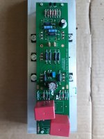
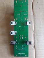
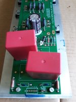
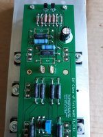
HI,Here I took a picture of the finished product. I lifted the diodes when I measured (ohmic), I didn't find the error. The coolers might be too small, but I'll fix that. The voltage is 5V higher at the Q2 drain.
Attachments
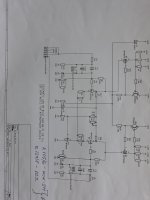

I can't see P2 on schematic, so it seems there is some info missing
though ........
is that exact pcb confirmed as working?
though ........
P2 has only the effect of allowing attenuation of the brightness of the on/off leds on the front panel. It allows matching of brightness in the event that the Led output is not matched, or allows them to be completely turned off (Yes, there are customers who want them off).
is that exact pcb confirmed as working?
Attachments
According to the attached diagram, P2 parallel resistance to R6 with which the dc offset is adjusted according to the instructions. I ordered the PCB from Mr. Csample from the forum and I had no doubts about the correctness. During testing, I connected P2 outside the PCB, with wires because I was changing resistors and finally ended up with a potentiometer at a value of about 10 Ohms. I checked the correctness of the PCB according to the schematic, but I did not notice a wrong connection anywhere. I'm already a little...
read service manual, written by Pa
P2 - you can toss it away, it's just a gimmick, having nothing with amplifier setting
now, again, did anybody made functional amp with these pcbs?
P2 - you can toss it away, it's just a gimmick, having nothing with amplifier setting
now, again, did anybody made functional amp with these pcbs?
Thanks for the effort. I say, I didn't doubt PCB at all. I saw some time ago on a forum that people sent pictures of such completed projects. I still have to search the forum, maybe someone with such experience will come forward. Thanks again and kind regards.
find connected thread and post link here
it's worth first having confirmed functionality of pcbs, then putting efforts in troubleshooting
I'm saying that simply because I didn't spot anything suspicious on your pics, so best to start from very beginning 🙂
it's worth first having confirmed functionality of pcbs, then putting efforts in troubleshooting
I'm saying that simply because I didn't spot anything suspicious on your pics, so best to start from very beginning 🙂
- Home
- Amplifiers
- Pass Labs
- F1 offset problem