.MODEL 2SK1058 NMOS...
.MODEL 2SJ162 PMOS...
OK, that is what I suspected.
The NMOS and PMOS models are essentially for IC Mosfets and are seriously unrealistic for power Fets. They produce wonderfully optimistic results.
Bob Cordell's book covers the basics on better models but he has done a lot of extra work since LTspice made further improvements on the internal calculation model.
His latest work, on DIYaudio, is the most accurate that I know.
Thanks for the offer, need to clear my PM mailbox first.
Best wishes
David
Last edited:
Have you links to alternative models? My searches have turned up nothing.
That said, I'd argue the structure of a lateral MOSFET is better modelled by the monolithic models rather than those developed for power (vertical) MOSFETs. The lateral structure is essentially exactly the same as that for a typical MOS IC process, just scaled up. The structure for a typical DMOS or HEXMOS FET is wildly different (hence the significantly better capacitances for the lateral parts and the significantly worse Rds).
This is what drew me to lateral MOSFETs in the first place. I was using 0.18um CMOS for my PhD work, and liked that the transistor structure for these big, slow parts is just about identical (albeit missing the gate silicide and other cool features of sub-micron processes) to the parts I was designing with.
More often than not, roughly 5 years ago, models from Onsemi, Fairchild etc. were crap, they were
often defective. andy_c here did some excellent work with a few bipolars, but I pointed out that
at high IB, Vbe was very large, from memory I think over 5 volts. I see some new work here at
Andy's site:
http://andyc.diy-audio-engineering.org/spice_models_intro.html
The older description on how he created those models:
http://andyc.diy-audio-engineering.org/spice_models_1.html
Bob Cordell did a pretty good assortment of parts downloadable here:
CordellAudio.com - SPICE Models
I mostly use Bob's models.
I enjoy following your work, was very impressed by how professional your last builds looked.
I don't know what Dave Zan will suggest, curious to see what he offers.
Last edited:
Thanks Pete. That's awesome. I substituted Bob's 2SK1056 and 2SJ162 models, and saw an increase in THD (400W, 4R load, 10KHz) to 2ppm. Rebiasing the output and redoing the compensation saw that come down to 1.6ppm.
That gives me confidence that the models are reasonably close - or at the very least out in agreement with one another 🙂
For reference, the component changes I made from the last schematic are:
R78: reduced to 15 Ohms
R28: reduced to 150 Ohms
R54: reduced to 47 Ohms
C7: reduced to 10 pF
That gives me confidence that the models are reasonably close - or at the very least out in agreement with one another 🙂
For reference, the component changes I made from the last schematic are:
R78: reduced to 15 Ohms
R28: reduced to 150 Ohms
R54: reduced to 47 Ohms
C7: reduced to 10 pF
Last edited:
Me too. I cast around the lab yesterday and went through a box of 100n 100V poly caps, measuring until I found 4 that measured 100n, then used them plus some 2K7 & 3K9 1% resistors to build a passive 1KHz twin-T notch.
Middle of the notch is at 1005Hz, but at 1000Hz (using a HP3325A as a source, so 1000.00Hz )it's still got plenty of loss , of 52dB.
That plus the nominally 95dB dynamic range of my HP3585B, plus the EOSC10KV3 oscillator that I'm building (something resembling 1ppm at 1KHz) should give me the tools I need to measure the actual amp.
Last edited:
Have you links to alternative models?...
Sure, I believe this is up-to-date http://www.diyaudio.com/forums/software-tools/266655-better-power-mosfet-models-ltspice.html?highlight=VDMOS but you may want to confirm with Bob directly and also ask about other threads.
I haven't used these models myself so I don't have any data on how accurate they are, just based on my read.
...structure of a lateral MOSFET is better modelled by the monolithic models rather than those developed for power (vertical) MOSFETs. The lateral structure is essentially exactly the same as that for a typical MOS IC process, just scaled up. The structure for a typical DMOS or HEXMOS FET is wildly different...
It will be educational to compare models intended for VDMOS with scaled up IC models.
The VDMOS models have quite a few parameters that can be tuned to match, even if they are not intended for Lateral FETs.
I look forward to your measured results.
Best wishes
David
Last edited:
Dave I thought that I read from Bob that his measured results were a bit better that
SPICE using the older models. This was as long as the output stage was the dominant
source of distortion. Don't remember where I read that maybe in his Hafler update.
SPICE using the older models. This was as long as the output stage was the dominant
source of distortion. Don't remember where I read that maybe in his Hafler update.
...plus the EOSC10KV3 oscillator...1ppm at 1KHz...
Can you test at 10 kHz? That's where your results surprise me and probably where limitations will show up most clearly.
Perhaps I should explain my surprise, I don't want to just criticize.
Your amp looks to have dominant pole compensation and the unity loop gain is around a reasonable 2 MHz so the feedback to control distortion at 20 kHz second harmonic is 40 dB, and less for 3rd and above, obviously.
So if you have circa 1 ppm distortion at 10 kHz then the open loop distortion of the class B output is only in the order of 100 ppm.
That seems extraordinary, even if the rest of the amp is essentially distortionless.
Have I misread your plots or made some other mistake?
Best wishes
David
Last edited:
...I read from Bob that his measured results were a bit better tha[n].. the older models
Yes that's my recollection too.
In comparison of old VDMOS with newer VDMOS, the new subthreshold conduction helps.
But Suzj has used the PMOS NMOS models so I am not sure how that comparison will work out.
Best wishes
David
Last edited:
Can you test at 10 kHz? That's where your results surprise me and probably where limitations will show up most clearly.
Perhaps I should explain my surprise, I don't want to just criticize.
I've bought components to run the oscillator at 1KHz for starters. I'll buy the components needed to run 10KHz as well, and use a switch (or perhaps a small-signal relay will work better) to switch between the two.
Your amp looks to have dominant pole compensation and the unity loop gain is around a reasonable 2 MHz so the feedback to control distortion at 20 kHz second harmonic is 40 dB, and less for 3rd and above, obviously.
So if you have circa 1 ppm distortion at 10 kHz then the open loop distortion of the class B output is only in the order of 100 ppm.
That seems extraordinary, even if the rest of the amp is essentially distortionless.
Have I misread your plots or made some other mistake?
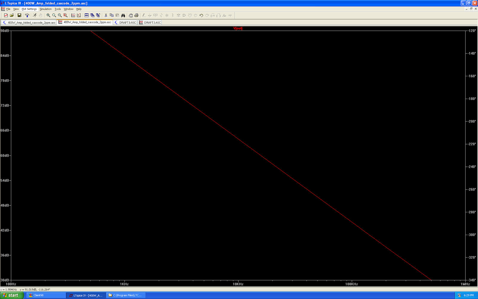
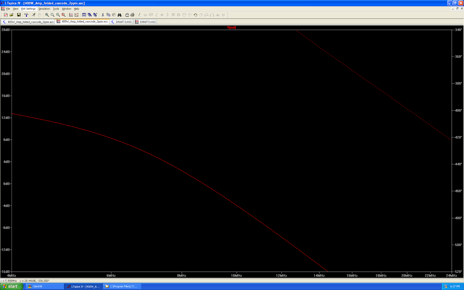
The LTspice plots are pretty terrible, with no grid. Using the crosshairs on the plot, I measure unity gain at 8.7 MHz (non-dominant poles are in effect before unity gain, so it's not at all unity stable, and if I continue my dominant roll-off to zero it hits at just shy of 20 MHz), and have 58dB OLG at 20KHz, 54dB at 30KHz. So therefore my open loop distortion is ~20dB worse than your guess, at something like 1000 ppm.
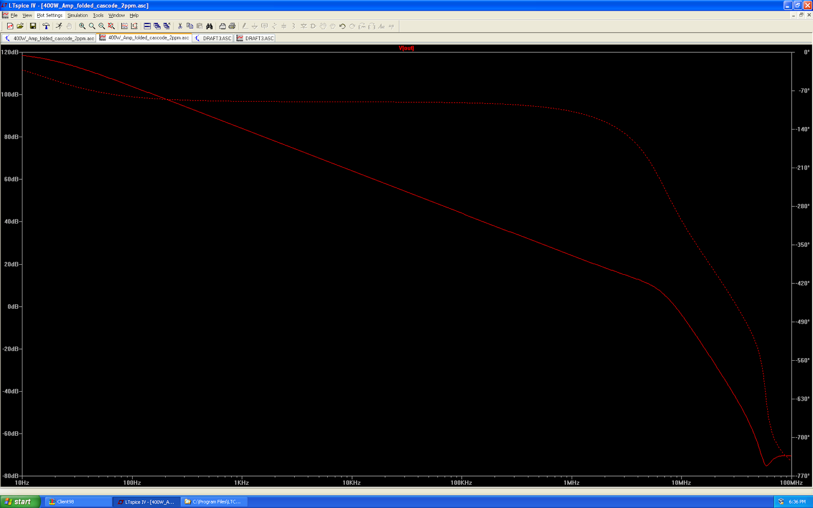
The LTspice plots are pretty terrible...
Isn't that your open loop?
If you have 20 dB of demanded gain, your loop gain is 20 dB less.
Another reason to use Tian, removes this uncertainty😉
It would also be useful if you turned the plot grid on.
Best wishes
David
Last edited:
The LTspice plots are pretty terrible, with no grid.
There is a grid probably black as your background. Go to Tools/Control panel/Waveforms and then change Color Scheme.
By the way black Background looks terrible to me, specially if you want to print it.
LTspice is excellent free spice software!
Last edited:
the open loop plots in Suzj's posts show crossing the 0dB with a steep slope.
I thought that the slope had to be less than -9dB/Oct at the zero crossing and preferably ~-6dB/Oct for improved stability margins.
Is Suzyj's open loop method correctly showing the 0dB crossing gain slope?
Similarly the phase at 0dB crossing is over 180° indicating that the amp oscillates. or does it?
Key here is that the amplifier doesn't run at unity (0dB) gain closed loop. When I close the loop, I've got 20dB (*10) gain. While it isn't stable at unity gain, it is stable (with ~70 degrees phase margin) with closed loop gain of 20dB.
You'll note the slope is 6dB/octave at the 20dB point.
You'll note the slope is 6dB/octave at the 20dB point.
...Similarly the phase at 0dB crossing is over 180° ... or does it?
You have confused the open loop with the loop gain, the similarity of name makes it a common mistake.
What SuzyJ has shown is the open loop but it is the loop gain that indicates instability
So I was fairly sure that the plot shown could not be a usable loop gain.
And it's the loop gain that determines the distortion reduction due to feedback.
That was the point of my previous post,
Best wishes
David
Last edited:
Key here is that the amplifier doesn't run at unity (0dB) gain closed loop. When I close the loop, I've got 20dB (*10) gain. While it isn't stable at unity gain, it is stable (with ~70 degrees phase margin) with closed loop gain of 20dB.
You'll note the slope is 6dB/octave at the 20dB point.
I think you are both confirming that to read the Suzyj plots one needs to look at the +20dB scale instead of the 0dB and work up from there.You have confused the open loop with the loop gain, the similarity of name makes it a common mistake.
What SuzyJ has shown is the open loop but it is the loop gain that indicates instability
That was the point of my previous post, and why I was fairly sure there was a mistake, the plot shown could not be a usable loop gain.
And it's the loop gain that determines the distortion reduction due to feedback.
Best wishes
David
Does it then follow that to read the gain available for NFB also needs 20dB to be subtracted?
Last edited:
Does it then follow that to read the gain available for NFB also needs 20dB to be subtracted?
Exactly so, this was my point in my post #52 to Suzyj's #51, the calculations are out by 20 dB.
I edited my previous post #56 to make this more clear but a little too slow.
Best wishes
David
Last edited:
"Final" schematic for the power PCB. I've included the various power supplies for the amp (+/-36V, +/-45V, +/-15V), plus a simple power-on mute circuit that uses DPDT relays to disconnect the gates of the power FETs on power up. I've never tried this previously - I've always put the relay in series with the speaker, but I figure it's worth a try.

Layout is fairly straightforward - feature sizes are dictated by the TPS7A49 & TPS7A30 SSOP low noise regulators, at 10 mil.
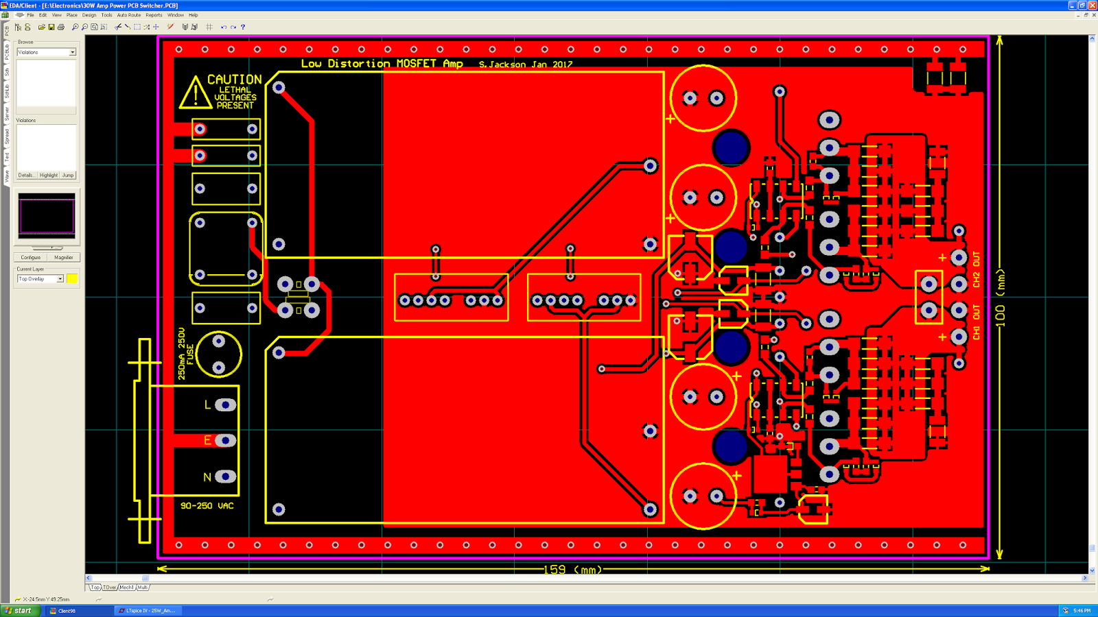
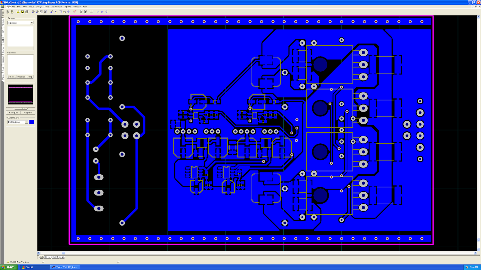
The whole thing fits neatly in a 160mm x 100 x 50 Hammond instrument case, with the signal PCB slotted in on top.
Layout is fairly straightforward - feature sizes are dictated by the TPS7A49 & TPS7A30 SSOP low noise regulators, at 10 mil.
The whole thing fits neatly in a 160mm x 100 x 50 Hammond instrument case, with the signal PCB slotted in on top.
Disconnecting the gates of mosFETs can leave the charge on the gate at some random value.
The FET could be fully on or Fully OFF or some intermediate level of conduction.
The relay should take the gate to some fixed level to ensure the conduction state is what you require.
The FET could be fully on or Fully OFF or some intermediate level of conduction.
The relay should take the gate to some fixed level to ensure the conduction state is what you require.
- Home
- Amplifiers
- Solid State
- Extending the AEM6000 design to ppm THD