Is a solution like this feasible? I've referenced the datasheet for the peak current, which indicates a rating of 9A. This suggests approximately 2.25A per channel, considering there are four channels. Unfortunately, due to the spacing between pins, the traces can't be wider than 0.07 inches (1.8mm). Recognizing this limitation, I've contemplated the idea of using traces that are 0.15 inches (4mm) wide, placed at the maximum distance possible between the pins of the IC. While I'm not certain if this is the optimal approach, it's the best solution I've come up with thus far.
I want to express my sincere gratitude for your valuable input. I greatly appreciate it. I'm feeling quite fatigued today as I just returned from the gym, so I'll continue with the editing tomorrow, following the method you've described. Thank you once again.

I want to express my sincere gratitude for your valuable input. I greatly appreciate it. I'm feeling quite fatigued today as I just returned from the gym, so I'll continue with the editing tomorrow, following the method you've described. Thank you once again.
Yes, it's ok, but it's only the easy part of the design because those tracks are straight and parallel 🙂.
The current flowing through the speaker is produce by the supply and flows though the chip; that means there are other tracks which handle high currents, not only the speaker ones. Current goes from positive side of the supply to Vcc pins of the chip then from the outputs of the chip to the speaker then return to the other output of the chip (they are paired) then to PWR GND pins of the chip then to negative side of the supply. As a consequence, the tracks connecting Vcc pins and GND pins of the chip to the supply should also be wide, theoretically wider than the speaker ones because they handle the sum of the currents flowing through the speakers.
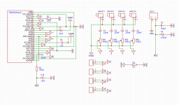
Could you post schematics ?. Before going to pcb design, you should ensure that the schematic is correct, at least electrically.
The current flowing through the speaker is produce by the supply and flows though the chip; that means there are other tracks which handle high currents, not only the speaker ones. Current goes from positive side of the supply to Vcc pins of the chip then from the outputs of the chip to the speaker then return to the other output of the chip (they are paired) then to PWR GND pins of the chip then to negative side of the supply. As a consequence, the tracks connecting Vcc pins and GND pins of the chip to the supply should also be wide, theoretically wider than the speaker ones because they handle the sum of the currents flowing through the speakers.
Could you post schematics ?. Before going to pcb design, you should ensure that the schematic is correct, at least electrically.

Could you post schematics ?. Before going to pcb design, you should ensure that the schematic is correct, at least electrically.
Hi, it's easier with the schematic !
AGND and GND should be routed separately, but should be connected together in a single point. The trick is to add a zero Ohm resistor on the schematic between AGND and GND. When populating the pcb with the parts, install a jumper in place of the resistor or a solder blob if you choose a smd resistor with a package such as a 0402
The ground to use at the inputs is AGND, not GND which is the power ground. You don't want to mix input signal with output.
Around the TB2929:
- Pin4 shouldn't be left open, connect it to Vcc through a 22k.
- Pin6 should be connected to Vcc. Place C5 close to the chip.
- Pin13 should be connected to AGND
- Pin22 shouldn't be left open, connect it to Vcc through a resistor with an ecap to GND, see DS page 4. There are not enough data on the DS to calculate the resistor. Try 100k and 10uF. Some tuning may be required. Don't install the cap for the first tests.
Could you please confirm if I have grasped the recommendations correctly?
AGND and GND should be treated as separate nets, each having its dedicated ground plane. The key is to connect these ground planes at a single point. To achieve this, a zero-ohm resistor can be used on the schematic, and when the PCB is populated, either a physical resistor (with very low resistance) or a solder bridge can be employed to make this connection.

AGND and GND should be treated as separate nets, each having its dedicated ground plane. The key is to connect these ground planes at a single point. To achieve this, a zero-ohm resistor can be used on the schematic, and when the PCB is populated, either a physical resistor (with very low resistance) or a solder bridge can be employed to make this connection.
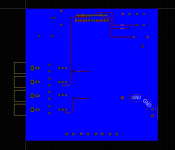
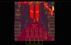
After dedicating three days to this endeavor and countless hours of contemplation, I've arrived at this design iteration. While I'm uncertain of its quality, I greatly value any insights or feedback you can provide. I've incorporated four volume controls, one for each channel, but I'm unsure if their connections are correct. Your assistance throughout this process has been immensely appreciated.
Attachments

Hi,
Congrats, good work for a first pcb! And thank you for the credit on the silkscreen.
There are still some improvements:
Congrats, good work for a first pcb! And thank you for the credit on the silkscreen.
There are still some improvements:
- Layout around the chip is not easy to do with two ground planes. Forget or reduce the Agnd one (blue). Agnd plan could be reduced to the area in green.
- Evacuate the 4 inputs pins (11,12,14,15) on the left of the chip (pin1) on blue side, switch to red side then make the 4 tracks going down under the green area. Also move C8 on the left, under the green area. By this way, all Agnd tracks will be on the left side of pcb.
- On red side, use a thick track between the two pins row of the chip, and connect all the GND pin. Then rotate C6 180° and swap pin 1&2 of VCC connector in schematic, this will allow you to route VCC and GND from the chip to C6 then to the connector with two thick traces without swapping side. If you prefer, route VCC and use a ground plane for GND.
- Those are suggestions, but you got the idea.
- Don’t forget to add 4 fixing holes in the corners.
- In addition, C7 R1 C6 and C9 are too close to the edge of the board, don’t forget the massive heatsink on which the chip will be attached.
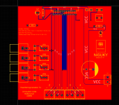
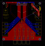
I believe the outcome of this PCB aligns with the insights I gleaned from your guidance. While I may not have comprehended every detail, I'm of the opinion that I have achieved an improved result when compared to the initial PCB design. What are your thoughts on it?
Attachments
Hi,
I think you're using web based EasyEDA, I'm not familiar with it. Did you post the right pics ? Most of the tracks, which were previously ok, are missing, and the green thing does not looks like a copper layer.
I think you're using web based EasyEDA, I'm not familiar with it. Did you post the right pics ? Most of the tracks, which were previously ok, are missing, and the green thing does not looks like a copper layer.
I am currently utilizing EasyEDA, albeit not the web-based version. I sincerely apologize for any confusion regarding the images. In my attempt to enhance the design, I inadvertently overlaid the soldermask layer, causing the tracks to become obscured. The green element was intended to serve as the silkscreen layer on the bottom. With these revised files, I hope to simplify matters and apologize once more for any prior misunderstandings.
EDIT:
I made several adjustments to the design. Firstly, I eliminated the ground plane surrounding the IC and introduced two opposing ground planes. The upper one, marked in BLUE, is designated as GND, while the lower one, indicated in RED, is designated as AGND. To ensure optimal conductivity, I widened the tracks connecting the IC's GND and VCC points. Additionally, I introduced a 0Ω resistor between these two planes for enhanced electrical flow. Furthermore, I relocated the four outputs to the side, as opposed to their previous position at the bottom.
Attachments
Last edited:
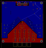
Great!
My last comments :
My last comments :
- C10 on the schematic, then of pcb, is not correctly located. Its place is after the resistor, not before. It is useless where it actually is.
- Speaker tracks will handle high current. When changing side, you use very small vias with very small surface, they're not suited for high current. Keep those tracks on component side (red). On the blue side, the ground plane is useless in the area, don't define this plane as a routing constraint, route the tracks freely.
- On top of the board between the chip and the board edge, the ground track could be much wider.
- C5 could be much closer to the chip and with short connections: install it on the left of the chip, close pin1
- Your thin tracks are too thin, make them wider, especially on pin13 which is analog ground.
- More is nitpicking. 🙂
I want to express my sincere gratitude for the tremendous effort and assistance provided by all of you who have contributed to both of my threads. Your valuable input and responses have not gone unnoticed.
Regarding the PCB:
At this stage, I am seeking guidance on the following:
What additional layers do I need to incorporate?
Once again, thank you all for your assistance and insights.

Regarding the PCB:
- The VCC main track has been set at 9mm.
- POUT, AGND and GND tracks around the IC have been spaced at 1.89mm.
- Remaining tracks have been adjusted to 0.5mm.
At this stage, I am seeking guidance on the following:
What additional layers do I need to incorporate?
Once again, thank you all for your assistance and insights.
Front/back/edge and front silk should be enough. EasyEda probably embed a wizard which produce fabrication files for JLCPCB, it's the same group with LCSC.
If any of you could spare a moment, I would deeply appreciate your expertise in reviewing my design. Please take a look and let me know if you spot any significant errors or issues. Your input is invaluable in ensuring a smooth fabrication process.
Thank you in advance for your time and assistance.
Warm regards,
Prognosis


Thank you in advance for your time and assistance.
Warm regards,
Prognosis
Hello,
The first comment in post#32 regarding C10 hasn't been processed. That should mute the chip during power up and avoid 'plop' in the speakers.
The first comment in post#32 regarding C10 hasn't been processed. That should mute the chip during power up and avoid 'plop' in the speakers.
I thought C10 should be located after R2, in the way my last PCB layout is (compared to layout in post #30).
R2 and C10 should change position with each other?
The PCBs were already manufactured, they were shipped yesterday... 🤣 I guess there's nothing I can about it now. I'll think of something when they arrive.
R2 and C10 should change position with each other?
The PCBs were already manufactured, they were shipped yesterday... 🤣 I guess there's nothing I can about it now. I'll think of something when they arrive.
There's no harm, it has no influence on amplifier operation, except power up. C10 has to be connected to pin22, on the other side of R2.
After the first tests of the amplifier, you'll decide what to do : leave it or solder it on the back side of the pcb to R2 and ground.
After the first tests of the amplifier, you'll decide what to do : leave it or solder it on the back side of the pcb to R2 and ground.
- Home
- Amplifiers
- Chip Amps
- Exploring the Toshiba 2929 Audio IC - Seeking Guidance