Hello ,,,Those days I’m trying to make a small solid state amp , and I found a nice orange amp crush 20L ,, but I will put another preamp section and I will keep only the power section from ORANGE … but I see strange things in the schematic . First strange thing it’s the voltage regulator where it goes to ground ( I spot with green mark ) .. the second it’s the FET ( spot with blue mark ) , the preamp section goes to the drain of FET , but why not go straight to the TDA2050 input ?
any answer could solve these strange things for me… thank you
any answer could solve these strange things for me… thank you
Attachments
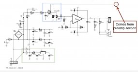
The FET looks to be used as a form of series switch (for muting) and is on when AC power is present. The 10meg/1uF on the gate set a time constant for the delay.
The 5v regulator is fine as far as it goes but the circuit does not show what the regulator powers. Maybe some front end circuitry/logic etc.
You can just use the TDA output stage without any of that extra stuff and feed the audio into the volume control which is correctly positioned.
The 5v regulator is fine as far as it goes but the circuit does not show what the regulator powers. Maybe some front end circuitry/logic etc.
You can just use the TDA output stage without any of that extra stuff and feed the audio into the volume control which is correctly positioned.

good morning and thank you for the answer .. and I am thinking of using the TDA section direct .. but why make it so complex ?!…. Thank you again my friendThe FET looks to be used as a form of series switch (for muting) and is on when AC power is present. The 10meg/1uF on the gate set a time constant for the delay.
The 5v regulator is fine as far as it goes but the circuit does not show what the regulator powers. Maybe some front end circuitry/logic etc.
You can just use the TDA output stage without any of that extra stuff and feed the audio into the volume control which is correctly positioned.
Only the designer knows why it is as it is 🙂 Without seeing the whole design it is impossible to say.
The other it’s just preamp section .. for the red mark I don’t know where it goes . It just say CN7 , maybe mean connection 7 … and the pin3 goes to pin1… that’s it..I thinking to start from the aux in section and I hope to work !
Attachments
That.
Personally I´m a minimalist and make stuff as simple as possible, as long as it works, but many designers love to add bells and whistles here and there, quite justified in this case because that muting circuit most probaly mutes or strongly attenuates turn-on "thump", which is annoying.
Besides, stuff is machine manufactured in robot factories and components are cjheap, so it´s easy to add them, no big deal.
This is NOTHING compared to some stuff being made today.
Part of the complexity is the polarity requirements for driving an n-channel JFET from the AC signal, requiring negative bias
to turn it off (hence the negative rail connection), and a zener to bring the voltage down (+ve voltage on the gate would
allow gate conduction).
It seems to have a time constant of 0.1s or so, followed by a 10s timeout due to the 10M resistor - it strikes me that the 1N4148
is connected in the wrong place, and should go to the FET gate so that it can be switched off rapidly on power going away, yet
retain the 10s time constant at startup for de-thumping purposes.
So the red mark is the muted section of amp ,,, I will skip it. going straight to the master volume… should I leave the pot the same or change it?Part of the complexity is the polarity requirements for driving an n-channel JFET from the AC signal, requiring negative bias
to turn it off (hence the negative rail connection), and a zener to bring the voltage down (+ve voltage on the gate would
allow gate conduction).
It seems to have a time constant of 0.1s or so, followed by a 10s timeout due to the 10M resistor - it strikes me that the 1N4148
is connected in the wrong place, and should go to the FET gate so that it can be switched off rapidly on power going away, yet
retain the 10s time constant at startup for de-thumping purposes.
I don’t have problem with poping speaker but thank you ..Starting Pop protection for amplifier
So must I replace the 1n4148 in front of gate and behind of 10M or parallel with 10M ?Part of the complexity is the polarity requirements for driving an n-channel JFET from the AC signal, requiring negative bias
to turn it off (hence the negative rail connection), and a zener to bring the voltage down (+ve voltage on the gate would
allow gate conduction).
It seems to have a time constant of 0.1s or so, followed by a 10s timeout due to the 10M resistor - it strikes me that the 1N4148
is connected in the wrong place, and should go to the FET gate so that it can be switched off rapidly on power going away, yet
retain the 10s time constant at startup for de-thumping purposes.
It’s complex but yes , it works like switch ( on / off ) signal or ground to master volume or something like that ,A bit confusing to me too. Is the regulator producing the artificial ground?
It all looks pretty conventional. Can't see any clues as to what the 5 volts is supposed to feed though. There must be more...The other it’s just preamp section .. for the red mark I don’t know where it goes . It just say CN7 , maybe mean connection 7 … and the pin3 goes to pin1… that’s it..I thinking to start from the aux in section and I hope to work !
It doesn't look to be doing anything at the moment tbh. The PSU input looks like an AC-0-AC input so conventional. Simple Zener shunt regs for the opamp supplies.A bit confusing to me too. Is the regulator producing the artificial ground?
Can you explain how this it works on this schematic ?It doesn't look to be doing anything at the moment tbh. The PSU input looks like an AC-0-AC input so conventional. Simple Zener shunt regs for the opamp supplies.
This schematic is flawed . Its too complicated . Theres really nothing in it . Rectifier is rectifying tda2050 is amplifing . Preamp is preamplifing . Thats it . Why you want the working can you explain what are your end goal .
Can you explain how this it works on this schematic ?
The split rail supply is conventional. This is from the web. 30 volts AC when rectified and smoothed generates approximately 40 volts DC. Calculated as Vac * root2 which is 30 * 1.414
So to get a nominal plus and minus 24 volts as in your circuit require an input of about 18-0-18 volts AC (approximately)
The Zener shunts are a common and good way of providing stable lower voltage rails. The Zener voltage set the rail voltage and the series resistor limits the current.
So guys I build the power amp section from aux-in with +15v and -15v on Opamp and goes direct to potentiometer .and I add my preamp in front of aux-in … working good!!!!!… tomorrow I’ll try the muted section ..I have an on other question .. this schematic of orange crush run with 8ohm speaker .. but I have 4 ohms speaker .. can I add an resistor 4 ohms/20 watt before the output ,, to make 8 ohms output ?
- Home
- Amplifiers
- Solid State
- Explain strange solid state schematic