Not at all! I know exactly how time consuming this part can be...Last, please, don't believe that the L.C. VSSA or my Diamond VSSA are primitive, because they look simple.
Even with my (very popular layout) symasym the final HF compensation layout took a whole month (with my speed... 🙂)...
BTW: is this DVSSA version already built by you or other or "just" in spice?
Yeah, that'd be great... I am really confused with the number of alternatives out there now...OS had a different approach, adding drivers or Baxandall VAS, with amazing results on the paper.
I am very passionate about the idea to compare the two approaches, in listening, to make myself a philosophical opinion.
I chose DVSSA vs one of SlewMaster CFA as a start because it (looks... 🙂) a simpler design.
I like to place it somewhere between the middle. Those number of trannies seems a bit too much for me
but thats why such a listening test would be great to compare if its only good in spice or makes a real difference.
Ok then I add these Cs to my sch/pcb, thanks!My point is to set the low pass filter C11/12, as i indicated.
Thimios: differences in sound with Krypton-ND related to a simple CFA-X..?
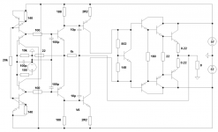
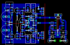
Schematic and PCB modded, including servo (can be placed as a 2 pole module as well to spare space).
Its very compact ~4 x 4cm + the servo as placed.
Any comments..?
Questions checking OS's similar solutions:
Schematic and PCB modded, including servo (can be placed as a 2 pole module as well to spare space).
Its very compact ~4 x 4cm + the servo as placed.
Any comments..?
Questions checking OS's similar solutions:
- Why to use double opamp servo?
- Is it better to lead it to the CCS..?
- What about those emitter degeneration resistors added by Pete at the "middle" stage?
Attachments
.... I couldn't get the distortion to simulate as low as Esperado...
Nor could I, I had a discussion with Esperado and I think the difference is because of the Cordell models rather than what Esperado used.
Your results tend to confirm that, but I don't want another controversy so I will note that there may be other causes.
For instance, you have a little different values of Output Inclusive Compensation from the version I have.
Have you checked the stability of that OIC loop?
Your test @ 2 watts @ 1 kHz is pretty easy and should look impressive on almost any amp, have you tried harder tests?
Full power @ 20 kHz should separate the serious units, it may even make the CFAs look better, relatively.
Best wishes
David
Last edited:
There's a bunch of such circuits, inspired by Nelson Pass F5, including the VSSA :How about one with only four...
http://www.diyaudio.com/forums/pass-labs/255523-recommendation-5-10w-amp.html#post3911652
http://www.diyaudio.com/forums/pass-labs/210538-f5-bjt-input.html#post2980905
http://www.diyaudio.com/forums/pass...riant-gr-grade-jfets-latfets.html#post3980775
Sony only upgraded my TSSA, VSSA is a step forward from TSSA. Acronyms speaks for themselves.if you want upgraded VSSA, look at Sonny's TSSA v1.7
Hi Guys
Esperado's site is very interesting. I think one of the best additions to the circuit he made was the RCs within the diamond.
Note that his THD tests are only for the first four harmonics, where most follow Bob Cordell's method using ten harmonics. One the Esperado's measurements makes a reference to ten harmonics, and the overall number is higher as expected.
All good stuff anyway.
Have fun
I had a boring controversy with a member of this forum about the distortions numbers in my article. I was said I don't used the good models for power FETs in my article.and the overall number is higher as expected
I don't worry to redo all the prints just to change by a factor of 2 the absolute numbers. All my articles are "comparisons". Whatever the power stage is, and even with perfect devices, as the input stage use correct models and the others the same, the relative distortions stay in the same direction or ratio between the two compared topologies.
About high order distortions, i doubt any one can hear frequencies higher than 40KHz ?
My IRL distortiometer filters what it measures in the 20 to 20 000 frequencies range.
This said, if somebody is making simulations from my files, it is recommended he uses the Cordell models, on his side. or, better build them and measure the real stuff ;-)
Oh, by the way, if somebody want to use this amp, and if you can afford the extra price, i recommend to double the number of power devices. Paralleling them reduce crossover distortion of the output stage further.
Last edited:
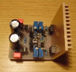
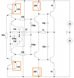
I just started to bringing it alive but (as usual... 🙂) it doesn't work (as I expected).
The schematic is attached. As you can see the PS is now just +-35V DC.
There is no OPS so the VAS is shorted and that's where the FB is driven from.
The orange-marked resistors are all 200R trimpots and for the start I set them all to 200R.
My initial strategy for the process was:
Reality:
The initial C values were: 100p @ input, 100pF after diamond and 10pF for VAS bases.
I increased them in hope for no oscillation but it didnt help.
Any idea?
The schematic is attached. As you can see the PS is now just +-35V DC.
There is no OPS so the VAS is shorted and that's where the FB is driven from.
The orange-marked resistors are all 200R trimpots and for the start I set them all to 200R.
My initial strategy for the process was:
- input shorted
- scope on the output
- 2 DMM on both of the 10R VAS to measure the VAS current
- process: increasing both CCS untill I get around ~10mA for the VAS
Reality:
- as I turn the CCS trims nothing happens, there is no current at the VAS...
- if I open the input the test signal gets amplified but just with an additional oscillation
- even a transient (taking one DMM off from the VAS 10R) drives this IPS to oscllation
The initial C values were: 100p @ input, 100pF after diamond and 10pF for VAS bases.
I increased them in hope for no oscillation but it didnt help.
Any idea?
Attachments
Last edited:
Hi Guys
It is not usually recommended to hang a cap to ground right at the base of the input transistor. This capacitance works with the internal capacitances of the BJT to form an oscillator. This is why a base-stop is placed here. The input low-pass filter is then isolated from the BJT parasitics.
Apart from that, the VAS may not be able to drive the 1k feedback resistor and may oscillate in the attempt to do so. Even a single EF would help here. You could try a standard EF configuration used for preamp outputs, just so the feedback loop can be driven properly, to allow testing the front end.
Have fun
Input cap: not clear where should I put the extra resistor?
FB driving: I had success with similar layout and for DC bias and also for small signal it should work.
Tomorrow I'll check the CCS current and the 2nd stage current.
FB driving: I had success with similar layout and for DC bias and also for small signal it should work.
Tomorrow I'll check the CCS current and the 2nd stage current.
Well, just emitter followers, if you are talking about the input device. The cap, paralleled with the parasitic one of the transistor just make this one highter and more linear. Forget, no issues with this.This capacitance works with the internal capacitances of the BJT to form an oscillator. This is why a base-stop is placed here. The input low-pass filter is then isolated from the BJT parasitics.
+1Apart from that, the VAS may not be able to drive the 1k feedback resistor and may oscillate in the attempt to do so.
What a strange idea to test an amplifier without its output devices ? Too we need a voltage source between the collectors of the VAS trannies ( ~1...2V) to adjust the power devices quiescent to 150mA. You could use a TLVH431 Shunt with 1K adjustable potentiometer.
About oscillations, in the finished amp, the Laterals are charging VAS with a gate parasitic capacitance of high value. How can-you expect the phases at HF to be the same without ?
First, yes, verify your CSS. The two first stages are supposed to be at ~1.5mA.
Last edited:
Hi Cortez
The base stop goes between the bases of the input devices and everything else that is currently tied to them. This won't change basic functionality but improves stability.
If you see a voltage drop across the emitter resistor of the current source, then the CS should be working and providing a current based on the voltage drop and the R value (Ohm's law).
Ideally both CSs produce identical currents and the VAS devices are biased on to conduct some current of a given proportion. In most CFAs the input BJTs and second-stage BJTs operate at similar if not identical currents to maintain similar junction voltages and temperatures. To that end, small REs are added to help balance things.
CSs have their own gain and frequency response and are a part of the audio path despite what some say. It may be necessary to shunt the base of the pass element to maintain an AC ground there.
In a pinch, the CSs can be replaced by a simple R to each rail just to see if the rest works. These are usually split with a filer at the junction to ground, and sometimes a zener added to hold the input voltage steady.
Have fun
Last edited:
+1CSs have their own gain and frequency response and are a part of the audio path despite what some say.
It is one of the advantages of this configuration, they are not in the loop.
Hi Guys
Gain does not have to be in the voltage domain to be a problem. The direct-connected shunt capacitance on "just an EF" is one that precedes current gain and transconductance, so there can still be issues.
Testing the front-end of an amp on its own is a pretty standard way to build and test a new design. You can do the same with the output stage, since it handles significant current and tends to fail catastrophically if it fails at all. Incremental testing limits the amount of circuitry to troubleshoot; limits the number of possible simultaneous faults there might be; and tends to reduce fatal power ups.
Have fun
Struth, hundreds of VSSA, First ones etc... builds without any stability issues. They all have a 100pF directly from base to ground as an input filter. It does not introduce any instability, on the contrary, it kills any overshoot due to excessive fast edges on square waves.
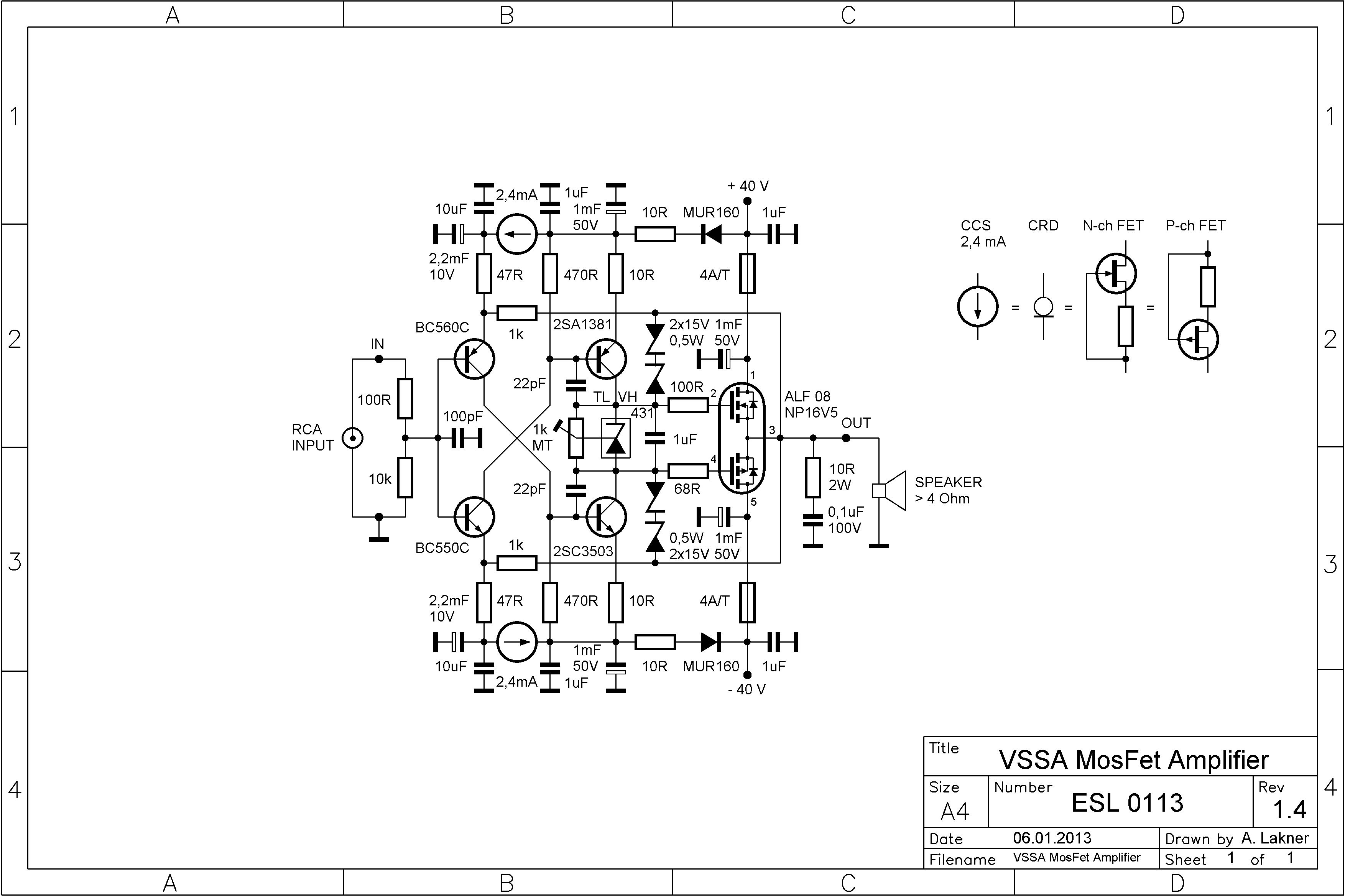
http://www.diyaudio.com/forums/atta...ssa-lateral-mosfet-amplifier-vssa-sch-1.4.jpg
A base/gate stopper is used to protect the previous stage from the capactive load.
http://www.diyaudio.com/forums/atta...ssa-lateral-mosfet-amplifier-vssa-sch-1.4.jpg
A base/gate stopper is used to protect the previous stage from the capactive load.
Hi Guys
Ubiquitousness does not equate to correctness.
Cortez has a build with oscillation and there are many reasons for that to happen. I simply pointed out one of them that is easily fixed - no need to be defensive. It is an irony that sometimes the very thing intended to stop oscialltion or RF breakthrough is the very thing to cause it and it happens frequencly even if it has never happened to you or me.
Have fun
I'm not (my poor English ?) , i just try to help.no need to be defensive.
This amp project has a 10MHz bandwidth. I had build one, working fine. At those frequencies any changes can be a problem, including the miss of the output stages ;-)
Don't read my inputs with others intentions.
I greatly advise Cortez to build-it full, with protecting resistances in the output stage, and we will see what's happens 🙂
I don't even know what output stages he want to add...
BJT ? I'm out of the game, not my project ;-)
Last edited:
Cortez, I realize that, indeed, you intent to use BJTs as output devices.
And that you gonna use two emitter followers to buffer the VAS before them.
You have to understand that such an amp will have no relationship with the DVSSA.
DVSSA was highly optimized in order to use the less active devices (poles) as possible. Here, you gonna replace very fast laterals by slower BJTs, and add two poles in the loop, not to mention that the needed temperature compensation can lead to added instability.
An entirely different amp, where everything need to be reconsidered. Including Miller compensation. Don't expect it to be that fast.
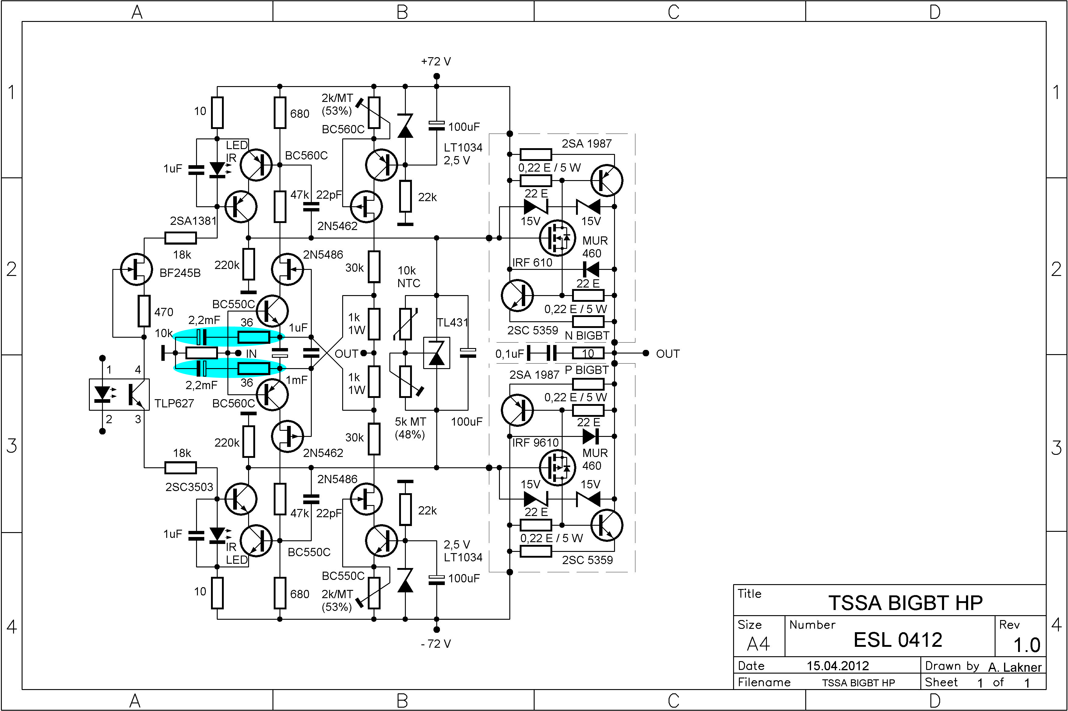
May-i suggest, to simplify your task, and if, for some personal reasons, you prefer BJTs, to use an existing output stage from OS, or inspire yourself from the BIGBT version of Lazy Cat ? http://www.diyaudio.com/forums/atta...plest-symmetrical-amplifier-tssa-bigbt-hp.jpg
There is good reasons why i preferred Laterals.
- They are fast
- They have a near infinite current gain at low frequencies.
- They are reliable and secure, because they don't suffer from secondary breakdown contrary to BJTs.
- They have a flat thermal point at ~150ma witch is a perfect quiescent for class AB, then a negative one at higher values. So they regulate themselves against thermal runaway and don't need any thermal compensations.
Some pretend MOSFETS are not so good than BJTs, on a sonic point of view, in the bass region, due to their relatively high RDSon. I don't agree: Damping factor is set by the feedback ratio.
Hoping this helps.
And that you gonna use two emitter followers to buffer the VAS before them.
You have to understand that such an amp will have no relationship with the DVSSA.
DVSSA was highly optimized in order to use the less active devices (poles) as possible. Here, you gonna replace very fast laterals by slower BJTs, and add two poles in the loop, not to mention that the needed temperature compensation can lead to added instability.
An entirely different amp, where everything need to be reconsidered. Including Miller compensation. Don't expect it to be that fast.
May-i suggest, to simplify your task, and if, for some personal reasons, you prefer BJTs, to use an existing output stage from OS, or inspire yourself from the BIGBT version of Lazy Cat ? http://www.diyaudio.com/forums/atta...plest-symmetrical-amplifier-tssa-bigbt-hp.jpg
There is good reasons why i preferred Laterals.
- They are fast
- They have a near infinite current gain at low frequencies.
- They are reliable and secure, because they don't suffer from secondary breakdown contrary to BJTs.
- They have a flat thermal point at ~150ma witch is a perfect quiescent for class AB, then a negative one at higher values. So they regulate themselves against thermal runaway and don't need any thermal compensations.
Some pretend MOSFETS are not so good than BJTs, on a sonic point of view, in the bass region, due to their relatively high RDSon. I don't agree: Damping factor is set by the feedback ratio.
Hoping this helps.
- Status
- Not open for further replies.
- Home
- Amplifiers
- Solid State
- Evolution of the VSSA? Esperado's DVSSA...