I mean if voltage output at the last tube is 2v divaided by the gain 18,3.. is 0,11v am I thinking wrong ?
Guess its not clear exactly what you are doing. The dac board in the picture has an opamp which operates the dac in voltage out mode. The opamp can output somewhere around a two volts RMS. In other words, 'consumer line level' output.
Regarding resistor I/V, the idea of using a resistor for I/V is not applicable to the dac board in the pic, not as it is designed anyway. Nor is the term all that useful in the context of ESS dac chips in general, since their output impedance is too low to work well with a resistor for I/V conversion. The dac chip would operate in some mixed-mode between current out and voltage out. However, since you don't seem to connecting a resistor directly to the dac chip's outputs, there can be no resistor I/V (unless of course its just not clear from the pic any mods you may have done). If there are mods then an overall connection schematic would be helpful.
OTOH the tube amp schematic has some resistors labeled with the letters R-IV. If you are simply referring to the resistors named that way and not their actual function in this case, that would be another matter.
Or if the dac chips outputs are connected to the tube amp inputs, then the larger the resistors, the more the dac chip is in voltage mode, not current mode. So its not exactly I/V anymore. Another thing to consider in that case is there is a LOT of RF noise coming out of the dac chip outputs (for these types of OS sigma-delta dac chips) that a tube amp might not like. Some people use a transformer between the dac outputs and an amplifier's input. The transformer may help a lot with filtering out that RF noise. That is, it may help more than a couple of passive RC filter stages.
Last edited:
The opamp is not to be used , I have removed the (smd) resistors betwen the ESS and The opamp,so I am going to connect the ESS to the input tube circuit.
Okay, thank you. IIRC the output impedance of an ES9038Q2M is somewhere around 800-ohms. Each output can be thought of as a resistor in series with a 3.3v peak to peak signal source with a +1.65v DC offset, more or less. So an R-IV in the tube amp would form a voltage divider with the dac chip internal resistance. Also, ESS recommends a very low impedance, direct ground path from the output stage back to the dac chip. Does that help at all?
So the 800 ohm internal resistans in paralell with 96 ohm (48+ 48 ohms) gets 85,71 ohm.
With 3,3 volts it draws 35mA ?
With 3,3 volts it draws 35mA ?
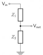
Its like the image below, where Z1 is more or less 800-ohms inside the dac chip.
Z2 is the net input impedance of your amplifier including any R-IV.
Vin is about 3.3v p-p, with a +1.65v DC offset.
Vout is the effective amplifier input voltage.
If your amplifier has a voltage gain of 18, or whatever it happens to be, and you want, say, +-10v out (assuming its capable of that), then that's 20v p-p out, right? So, to get full output you would need (20v p-p)/(18) volts p-p at the input. Calculate Z2 accordingly.
Attachments
Last edited:
If you try it, you will likely find its pretty close to the way I described it.
OTOH, there were older dac chips that were probably more suitable for resistor I/V. They had high-impedance outputs so they could force current through a small resistor. There are some various dac chip output architectures. For example, one type uses switched resistors (like ESS does). Another way is to use switched current sources. The latter way is better for resistor I/V. For better or for worse, its apparently possible to get better measurements using switched resistors. Dac chip sales in the mass market tend to be driven by some combination of favorable measurements and low cost. ES9038Q2M offers the potential for excellent measurements (using opamp I/V) at an attractive price point.
OTOH, there were older dac chips that were probably more suitable for resistor I/V. They had high-impedance outputs so they could force current through a small resistor. There are some various dac chip output architectures. For example, one type uses switched resistors (like ESS does). Another way is to use switched current sources. The latter way is better for resistor I/V. For better or for worse, its apparently possible to get better measurements using switched resistors. Dac chip sales in the mass market tend to be driven by some combination of favorable measurements and low cost. ES9038Q2M offers the potential for excellent measurements (using opamp I/V) at an attractive price point.
Last edited:
- Home
- Source & Line
- Digital Line Level
- ESS3038Q2M from Ebay