Hi Mark,
I can only speak for myself, but I've taken my 9038k2m as far as I care to. My initial goals were to put together an inexpensive decent sounding Dac with a few easy mods and I believe that I have achieved my goals. It may not be the best Dac out there, but it's good enough. Plus it's all in a nice serviceable case. As a non EE without tools and background I realistically can only execute simple modifications. That plus escalating costs and diminishing returns dictated where I stopped modifications. This excellent thread has evolved to become over my head at this point, but I did learn a lot. Thanks for all you've done.
Paul
May I ask for a show of hands if anybody is still working on modding the ES9038Q2M boards? ....
.
Mark, as it was mentioned some time ago, then upon the "full" mod only DAC chip remains (and some connectors perhaps). so at the moment I am working on a PCB layout based on the knowledge from this thread. just for fun of course 🙂
USB only. discrete regs for analog and a bunch of LDO for digital part. dedicated amanero socket and galvanic isolation perhaps. socket for I2C lines, so Arduino control will be indispensable. unfortunately not so much time for these activities nowadays ...
btw, still pretty happy with ES9028pro mod board. old vinyl rips to DSD128 sound so sweet ..
Hi Mark,
I can only speak for myself, but I've taken my 9038k2m as far as I care to. My initial goals were to put together an inexpensive decent sounding Dac with a few easy mods and I believe that I have achieved my goals. It may not be the best Dac out there, but it's good enough. Plus it's all in a nice serviceable case. As a non EE without tools and background I realistically can only execute simple modifications. That plus escalating costs and diminishing returns dictated where I stopped modifications. This excellent thread has evolved to become over my head at this point, but I did learn a lot. Thanks for all you've done.
Paul
Hey Paul,
How far did you go with it?
Mark, I still have my 9038Q2M board waiting to be played with. I just need to get some more pressing projects out of the way..
John
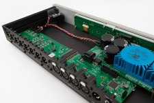
I added a decent linear supply(+/_15v), upgraded the opamp, increased the capacitance on the onboard power supplies, and added xmos based USB input. Put every in a decent case instead of peices on plywood so I can safely use it anywhere. It sounds good. If doing more than that costs and risk begin to rack up and you can buy a professionally designed/built Dac like the JLSounds Dac that definitely sounds better. But if you like to play, then the costs are just part of the hobby.
Paul
Paul
I’m still making my way through modding this board. So far...
ALW Jung Regs for original I/v stage and for avcc L and R
LT1763 regs for dvcc, vcca and the clock. Plus a larger cap on Dvdd .
Next steps will be a new clock and a new I/v stage with 3 opamps
ALW Jung Regs for original I/v stage and for avcc L and R
LT1763 regs for dvcc, vcca and the clock. Plus a larger cap on Dvdd .
Next steps will be a new clock and a new I/v stage with 3 opamps
Is this an improved (better) version?
ES9038 Q2M DAC DSD Decoder Board Supports IIS DOP 384KHz DSD512 + OLED | eBay
ES9038 Q2M DAC DSD Decoder Board Supports IIS DOP 384KHz DSD512 + OLED | eBay
May I ask for a show of hands if anybody is still working on modding the ES9038Q2M boards?
Obviously, I still owe some more work trying to simplify getting best performance when using AK4137 with ES9038Q2M. However, in the best case it would involve some additional fabrication of circuitry and register programming with Arduino or other MCU. Still interest in adding more complexity to the project in return for better sound quality?
Kayata might be the only one, seems like.
Just trying to gauge the level of interest to help me think about prioritizing activities.
I'm still modding Mark, I had a bit of a set back with the crystal replacement, resulting in ruining a Crystek and damaging the board to the point that the DAC chip got too hot. I've removed all the voltage regs, caps from the board and I'm awaiting a replacement which hopefully will be here in the next week or so.
I've built a few Salas regs. to supply +/- 15v and a 3rd for a low noise 5v whilst waiting so for the replacement so should have all power sources sorted for the DAC board as well as the AK SRC.
Is this an improved (better) version?
From the appearance it has digital switching to allow two different I2S input sources. Of course, that extra digital switching may add some jitter. Otherwise, it looks about the same as older boards in terms of functionality. What the ground plane looks like on the back side is important for our purposes here, since we rely on that for some of our mods. It may have changed significantly. Perhaps we will know more eventually if someone gets one and posts a pic of the back. Also, we don't know of the J1, J2 two jumper trick will stop I2C bus to make register access easier.
...had a bit of a set back with the crystal replacement, resulting in ruining a Crystek and damaging the board to the point that the DAC chip got too hot.
Wow, sorry to hear about that. If you get stuck in the middle of trying to do something and you post here we will definitely try to help you recover before its too late.
Most things that go wrong can be fixed, but I will admit that clock replacement requires some combination of very exact placement and careful process planning, and maybe some luck on top of that.
I find it gets a little easier as I work to refine the process of how I do it. Good lighting, magnification, small solder iron tip size, small diameter solder, extra paste flux, etc. all help. A dry run with the solder iron heat turned off may help. So might tinning the bottom of clock solder pads with small raised beads of solder all exactly the same size on each pad. Helps hold the clock up a little off the board so that added solder can penetrate under and melt the pre-tinned beads.
From the appearance it has digital switching to allow two different I2S input sources. Of course, that extra digital switching may add some jitter. Otherwise, it looks about the same as older boards in terms of functionality. What the ground plane looks like on the back side is important for our purposes here, since we rely on that for some of our mods. It may have changed significantly. Perhaps we will know more eventually if someone gets one and posts a pic of the back. Also, we don't know of the J1, J2 two jumper trick will stop I2C bus to make register access easier.
It's said that separate digital/analog power supply with ultra-low noise LDO (I read Chinese)

It's said that separate digital/analog power supply with ultra-low noise LDO (I read Chinese)
Okay, that prompted me to take a closer look at the corner where the power comes in. Looks like they added 2 more power terminals, but kept the 5v or 8v regulator, and added one more 3.3v regulator. To fit in the smaller space left over, looks like the 3.3v regulators are 5-leg varieties, which leaves open a lot of possibilities. Most likely only a rather small bit better than before in terms of power supplies. Best to replace all the regulators for the dac chip and clock. AVCC_L, AVCC_R, VCCA, DVCC, and Clock. The first two are the most critical to start with of course. Good to keep the MCU and display on its own separate regulator, presumably one of the existing ones.
If we could see one up close, top and bottom, we might figure out a little more detailed understanding of exactly what they did.
Thanks Mark,Hi Anton,
You seem to have the right basic idea. R6 and R7 form part of the input filter time constant so you need to know what those are. Or perhaps you could buffer the octodac output first with two more opamps, but that gets to be a lot of opamps in the signal path.
AD797 that Monte suggests is very nice opamp, but one no longer used by ESS for output stages. AKM and ESS both now use OPA1612. The reason on the ESS side, at least, is because of the 'ESS hump' issue. Seemingly, it turns out nobody found a way to reliably solve it if using AD797 for the output stage (although AD797 still makes for a really good AVCC buffer).
Some discussion on the ESS hump and opamp selection can be found at ASR: ESS THD ‘Hump’ Investigation | Page 14 | Audio Science Review (ASR) Forum
Also, its possible if the DC offset from the I/V converter stage is already removed at octodac outputs, then AD797 might be okay for differential summing/filtering use, not sure. If the offset is removed, it might be helpful to know of it was done as described at ASR or if DC blocking caps are used, and also if there are equivalent output resistances more or less the same at R6 and R7 in the schematic you posted .
In addition, I personally would be concerned if octodac had no MCU at all. It could be controlled over I2C by the XMOS chip or some other part that might not be recognized as performing what would normally be the MCU function.
Then I believe the right way would be to receive the DAC8 and then check for what kind of resistors are used there. I have also asked Okto the same question as here and currently awaiting for reply.
Regarding the new updated boards, I guess they may use the XMOS chip to control the sabre chip. Here is what Pavel replied me regarding this:
The DAC8 PRO has a next-gen board, without an on-board MCU (so no Sabre chip settings) and is not designed to be DIY friendly.
Modifying the DAC8 PRO would be possible I guess if the I2S lines from the input board were disconnected and tapped into. We could provide support, but it might require some debugging on your side in the process and there is a risk of running into problem that cannot be solved remotely.
So we agreed that modifying the DAC8 and integrating the MINIsharc is not a very good idea. Instead I was advised to use a PC based software crossover with e.g. Jriver and Audiolense and I am quite interested in this solution to be honest. Still, I will have to find the way how to convert the balanced signal to unbalanced.
Yes, this is obsolete, the new board is different as I mentioned above. There are some pictures of the new board Vs old:Okto Dac8 module manual: https://www.oktoresearch.com/downloa...ule_manual.pdf
Page 5 shows the I2S input connector. That's what I would want to interface to Sharc.
Review and Measurements of Okto DAC8 8Ch DAC & Amp | Page 33 | Audio Science Review (ASR) Forum
There are some pictures of the new board Vs old...
Okay, I see the new picture. Makes it look easy to get into the dac chip via I2S (or possibly SPDIF, since I can't read the connector labels) since all the I2S (and or SPDIF) lines go through a connector down to the XMOS and AES intput board. Just a matter of tracing out the correct lines and tapping into them. Also, I would see if the I2C lines go through that same connector. If so, great. If they did something stupid like grounding the dac chip I2C pins right at the chip, then not as good. In any case you would need an ES9038PRO data sheet to work from, if thinking of doing any customization.
Attachments
Last edited:
Wow, sorry to hear about that. If you get stuck in the middle of trying to do something and you post here we will definitely try to help you recover before its too late.
Most things that go wrong can be fixed, but I will admit that clock replacement requires some combination of very exact placement and careful process planning, and maybe some luck on top of that.
I find it gets a little easier as I work to refine the process of how I do it. Good lighting, magnification, small solder iron tip size, small diameter solder, extra paste flux, etc. all help. A dry run with the solder iron heat turned off may help. So might tinning the bottom of clock solder pads with small raised beads of solder all exactly the same size on each pad. Helps hold the clock up a little off the board so that added solder can penetrate under and melt the pre-tinned beads.
Thanks Mark, when I meant the DAC chip got too hot, I mean I tried to reverse the situation and replace the crystal with the original. I soldered four wires on the crystal and then soldered back to the points on the board, this didn't work as the DAC chip suddenly turned into a little heater and became too hot to touch in seconds.
I'm not happy with myself as I had the solder, flux, braid, x2 magnifier, LED lighting, flat tip small tip and I still managed to screw it up!
In hindsight, I should have soldered small solid core wires to the four points on the Crystek as the solder pads on the Crystek don't 'wrap' around to the sides making it a little difficult to apply heat.
Yep, prep and practice is key!
There was this new one that appeared the other week.....
NEW ES9038 ES9038Q2M DAC Decoder board Support IIS DSD 384KHz hifi Digital audio | eBay
NEW ES9038 ES9038Q2M DAC Decoder board Support IIS DSD 384KHz hifi Digital audio | eBay
There was this new one that appeared the other week.....
"Bidding has ended on this item."
I soldered four small solid core wires to my crystek and then planned on tacking those wires to the board. While adjusting the wires, the landing on the crustek came off! It looked like it was a goner. I managed to remove the top and solder to the edge of the board with a non solid core wire in the end. I was lucky.
"Bidding has ended on this item."
I haven't seen another on eBay so had to find the sold item.
Here's the AliExpress one:
ES9038 Q2M DAC PCM DSD Decoder board Support IIS DSD Coaxial Fiber input 384KHz DOP with OLED T0012-in Amplifier from Consumer Electronics on Aliexpress.com | Alibaba Group
I soldered four small solid core wires to my crystek and then planned on tacking those wires to the board. While adjusting the wires, the landing on the crustek came off! It looked like it was a goner. I managed to remove the top and solder to the edge of the board with a non solid core wire in the end. I was lucky.
Sounds remarkably familiar, prised the top off and then trying to solder a wire something the size of a human hair!!!!
- Home
- Source & Line
- Digital Line Level
- ES9038Q2M Board