enclosure is vented I believe. I’ve found shields on V1 especially in Phono to be always advisable if going for best measured resultsThe valves/tubes are in a closed metal enclosure, so no need to do extra shielding.
Seems you have a suggestion in mind... what is it?There is honestly only so much to get out of this topology. It can be pushed pretty far, but at some point you might want to go for something different.
The riaa is tricky... easily changed by a few picofarad.
Yes but I was able to attain .1db with selected triodes without deviation from the values indicated above.
Jfets from the same batch tend to exhibit similar characteristics. Mosfets however are a different story... From my experience there will be far greater potential variation between input 12ax7 triodes than the jfets.
Correct but you are assuming ideal circuit and properly selected JFETs. Given the valve quality in these devices it’s not a stretch to assume non-ideal JFETs or that they’re implemented in a way that could be improved upon. Chinese clones aren’t known for their build quality, attention to detail or similarity to the production schematics they’re scamming. Anyhow, it’s the piece of the puzzle with the least known info so I find it worthwhile to investigate even for the sake of curiosity.
Again, V1 shield helps in this regard.What is the psu transformer like? The original ear834p was quite modest. Be happy you have no hum.
Likely a 50VA toroid. A larger toroid would increase mechanical hum likelihood, not reduce it. Hum is best mitigated through attention to grounding practices or installing a snubber to reduce ringing.
Honestly, if it sounds good, don‘t mess it up too much. If it is really not good enough, think about a different topology...
Good advice but this is diyaudio after all, he’s engaged in the learning process.
There’s value in his interest.
Hi space
The original ear834p enclosure was not vented. But I am certainly not against using shields. I have some nice soviet sockets with shields here, but I would need a very pressing reason to de-solder the originals and solder in new ones with shields.
The problem with the few picos making a difference means that layout is really important. You can easily add a few picos on a circuit board alone by doing nothing and you might never know it. If you are getting even within 0.5dB of RIAA (measured using a good inverse RIAA network and frequency analyzer) then you are doing pretty good imho. Excellent job. I would gently note that passive RIAA is also easy enough to do and moves you into the nano farad range.
Also, as your input ecc83/12ax7 ages, your once close RIAA tolerance is sadly bound to drift. Swap the ecc83/12ax7 out for a new one and you will never know how good the close RIAA tolerance is. Maybe it is "good enough for rock and roll" though. I suspect most people just get used to a certain "sound" and are happy. That's fine too.
I don't know if others experience this, but measuring ecc83's on my digitally calibrated AVO MKII is honestly not such a treat. It is not easy to find ones that closely match channel to channel on transconductance. Such small ma/V values require lots of concentration. Amplification factors vary also channel to channel. I mention this since I found "tube rolling" really necessary with this circuit, but also found the need to closely measure them before hand, which was quite tedious. The ecc83/12ax7 is indeed very linear and an excellent voltage amplifier. However for the first stage in a one step RIAA correction it should be a well selected example (again just my opinion).
Sorry that you misunderstood my question on the power transformer. It has nothing to do with hum. I was only commenting that no hum is nice to have for what looks like a very faithful clone of this phono amplifier.
The question of the power transformer was in order to see what other PSU possibilities he might have. If it is a modest low VA torroid feeding a voltage doubler (as in the original ear), then major changes to the PSU will be a challenge. That is a pity since I experienced a significant improvement with this circuit was after improving the PSU.
IMHO there are better approaches to RIAA - but all with their own merits and costs. This circuit is definitely fine to start with and of course this is a diyboard. I am glad we agree on that.
Ian
Last edited:
Thanks to work, I had no time at all yesterday to get any work done on the amplifier. When I do, I will take a look at the toroid... I have witnessed many an unmarked Transformer in Chinese Amps though...
Sorry for keeping you waiting. Whenever I think that I have got a speck of time, brand new problems jump up and materialize themselves left and right. I actually got the amp done last week in about two short evenings, but I initially had the plan to only post when I had the schematic ready. I haven't completed it yet, but it's pretty far along. I will finish it one of these days, I hope.
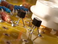
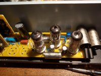
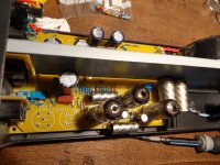
1) The FETs are indeed cascoded with V1, they are the first thing the input signal goes through. Sadly, as you can probably make out from the photos, there is no information whatsoever on them.
2) The Power Transformer does have some numbers on it, but it's jibberish. Judging by the size, it should be 50VA.
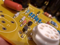
3) The many little resistors are in series and together form the load resistor of V2. It seems to be about 110k short of the 330k given in the original schematic. What a really ridiculous move to alter the board for a few cents saved...
4) I am an idiot starting work without proper desoldering equipment. Had I spend a few bucks more, I would have been finished in half the time.
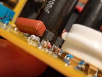
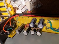
5) I changed a few cathode resistors to Amtrans and the RIAA to Shinkoh, the cathode resistor of V2 to an Elna Silmic II (ended up not bypassing that with 1uF...), all the Caps of the B+ PSU to Panasonic 100uF 400V bypassed with Panasonic 1 uF film caps, the diodes of the B+ supply to Vishay Ultra Fast Recovery Soft Switching and the coupling caps between V1 and 2 as well as V3 and output against Mundorf Zn. The RIAA caps were substituted with Charcroft Silver Mica of the same values. I removed the resistors and caps between V2 and 3 and the one from there to ground and substituted a 100R Allen & Bradley Carbon Comp. I found so many people who did this mod and nobody wrote about any problems with it.
The amp sounds noticeably different, I would say. Where it was good before albeit maybe lacking emotions a bit, it is now sparkly and alive.
I still think, this little amp is one of the best deals in hifi at the moment. A few little tweaks might make it something really sweet and worth having.
1) The FETs are indeed cascoded with V1, they are the first thing the input signal goes through. Sadly, as you can probably make out from the photos, there is no information whatsoever on them.
2) The Power Transformer does have some numbers on it, but it's jibberish. Judging by the size, it should be 50VA.
3) The many little resistors are in series and together form the load resistor of V2. It seems to be about 110k short of the 330k given in the original schematic. What a really ridiculous move to alter the board for a few cents saved...
4) I am an idiot starting work without proper desoldering equipment. Had I spend a few bucks more, I would have been finished in half the time.
5) I changed a few cathode resistors to Amtrans and the RIAA to Shinkoh, the cathode resistor of V2 to an Elna Silmic II (ended up not bypassing that with 1uF...), all the Caps of the B+ PSU to Panasonic 100uF 400V bypassed with Panasonic 1 uF film caps, the diodes of the B+ supply to Vishay Ultra Fast Recovery Soft Switching and the coupling caps between V1 and 2 as well as V3 and output against Mundorf Zn. The RIAA caps were substituted with Charcroft Silver Mica of the same values. I removed the resistors and caps between V2 and 3 and the one from there to ground and substituted a 100R Allen & Bradley Carbon Comp. I found so many people who did this mod and nobody wrote about any problems with it.
The amp sounds noticeably different, I would say. Where it was good before albeit maybe lacking emotions a bit, it is now sparkly and alive.
I still think, this little amp is one of the best deals in hifi at the moment. A few little tweaks might make it something really sweet and worth having.
Attachments
Tons of cheap transistor testers out there:
B1 Color 1.8" TFT ESR Meter Transistor Resistor Diode Triode Capacitor Tester | eBay
Can help identify the parameters.
Thanks for the photos.
B1 Color 1.8" TFT ESR Meter Transistor Resistor Diode Triode Capacitor Tester | eBay
Can help identify the parameters.
Thanks for the photos.
I seem to remember having seen a picture where the markings could be read. 2SK118 if memory hasn't failed me.
Last edited:
Thanks for your recollection.
I wonder what grade / target idss.
Are you referring to the production 834p or Douk clone?
I wonder what grade / target idss.
Are you referring to the production 834p or Douk clone?
It was the production 864 model.
I have these 2 pictures. Not great. But, perhaps GR.
DSC_8680.jpg - Google Drive
DSC_8681.jpg - Google Drive
Mogens
I have these 2 pictures. Not great. But, perhaps GR.
DSC_8680.jpg - Google Drive
DSC_8681.jpg - Google Drive
Mogens
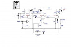
If I am looking at the values and corresponding it with the OPs trace correctly, then there 2x 2.2K and 2x 1.5K.
The 1.5K resistor is connected to the gate of the FET and the 2.2K is connected to the cathode of V1?
Edit: I located someone elses attempt at a rough schematic:

Apparently the Tant the OP removed was bypassing the 330K?
(Click image for higher res)
Although that seems pretty high for B+ from what I have seen elsewhere. I don't follow his chicken scratch well. Can anyone make sense of it?
It's an extremely strange layout, maybe for cost concerns but maybe also a plot on TDPs part to drive us all nuts ;-)
The 1.5K resistor is connected to the gate of the FET and the 2.2K is connected to the cathode of V1?
Edit: I located someone elses attempt at a rough schematic:
Apparently the Tant the OP removed was bypassing the 330K?
(Click image for higher res)
Although that seems pretty high for B+ from what I have seen elsewhere. I don't follow his chicken scratch well. Can anyone make sense of it?
It's an extremely strange layout, maybe for cost concerns but maybe also a plot on TDPs part to drive us all nuts ;-)
Last edited:
3) The many little resistors are in series and together form the load resistor of V2. It seems to be about 110k short of the 330k given in the original schematic. What a really ridiculous move to alter the board for a few cents saved...
I meant V1. They make about 220k at the anode of V1....
Although that seems pretty high for B+ from what I have seen elsewhere. I don't follow his chicken scratch well. Can anyone make sense of it?
It's an extremely strange layout, maybe for cost concerns but maybe also a plot on TDPs part to drive us all nuts ;-)
The scratch Looks almost like what I drew up.. Except that the 1M resistor is 330k on my board. And the cathode resistor of the FET is 2,2K.
Last edited:
Can you clean up what you have and post?
220k may be reduced to account for the JFET?
There’s a difference between cheap and stupid. There’s a reason for it.
220k may be reduced to account for the JFET?
There’s a difference between cheap and stupid. There’s a reason for it.
Last edited:
I'll post it as soon as I get home and have a minute. I'm certain there's a reason for the reduction of the load resistor to 220K. But I don't think there is one for constructing it of 6 cheap smaller MFRs except "practical reasons".
Here's what I have. The part between V2 and V3 and the RIAA are obviously already changed to the modded version, as are the PSU capacitors and their bypass. I didn't bother to change any of it back, because the board is true to the original schematic there (first page, first post). The main thing is the input stage, and this I think is halfway acurate. The one resistor I couldnt properly identify by the color codes and also readings on the meter changed towards bigger values. Maybe it's 330k, maybe it 440k, maybe its even more.
Attachments
IIRC check out GoodSoundClub - Romy the Cat's Audio Site. This is Romy the cat's site and look up "end of life phono stage" i believe he modded an EAR unit to max performance. Perhaps you can find some good info.
The JFET should not be critical(*). Most any JFET will give a noise-figure at 1mA lower than the 2.2K source resistor, which is not large compared to the pickup noise impedance. 2.2K will also swamp-out JFET transconductance variation. I'd just use the same type and lot for both side of a stereo.
(*) That last plan can not be right. Assuming high voltage supply (over 70V), it runs the JFET at half the supply voltage. So for 200V supply, 100V, across a device rarely rated much over 35V. A 330K:68K divider might be OK for lower B+. 330K:33K may be even safer. There's no reason for more than a few volts across the FET.
(*) That last plan can not be right. Assuming high voltage supply (over 70V), it runs the JFET at half the supply voltage. So for 200V supply, 100V, across a device rarely rated much over 35V. A 330K:68K divider might be OK for lower B+. 330K:33K may be even safer. There's no reason for more than a few volts across the FET.
Hi
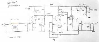
I just purchased the 834 clone kit, and I took some time to trace the PCB. According to the above thread and my portable analyzer, this is what I get.
Notice the plate resistor is 36k series to make 216k. This technic was used on the older 834P model, which the plate resistor is 56k series to make 330k.
The only issue is the MC step. I cannot find the miniature size to fit this PCB.
cheer
Coffin
Have a read of these 834 mods by Thorsten Loesch. https://www.audioasylum.com/message...ch-non-definitive-ear-834p-modification-guide
I've modified an 834P and scratch-built two. One of the Thorsten mods, I didn't try this, is to delete the cap between second and third stage. This will require changing the resistor in the third stage's cathode (the cathode follower resistor) if you retain the 12AX7 or leaving it the same and using a 12AU7 or 12AT7 (AT7 would be my choice).
I also had to use ferrite beads on the input wiring as close as possible to the board to kill RF interference.
Thorsten recommends Stevens & Billington TX103 MC transformers but I bet these wouldn't be cheap.
My preference would be external MC transformers to get them away from the preamp electronics and also use ones with multiple ratios you can set e.g. 1:5 and 1:10 or 1:10 and 1:20 step-up ratios.
I've corrected your schematic, see attached,
Steve
Attachments
Have a read of these 834 mods by Thorsten Loesch. https://www.audioasylum.com/message...ch-non-definitive-ear-834p-modification-guide
I've modified an 834P and scratch-built two. One of the Thorsten mods, I didn't try this, is to delete the cap between second and third stage. This will require changing the resistor in the third stage's cathode (the cathode follower resistor) if you retain the 12AX7 or leaving it the same and using a 12AU7 or 12AT7 (AT7 would be my choice).
I also had to use ferrite beads on the input wiring as close as possible to the board to kill RF interference.
Thorsten recommends Stevens & Billington TX103 MC transformers but I bet these wouldn't be cheap.
My preference would be external MC transformers to get them away from the preamp electronics and also use ones with multiple ratios you can set e.g. 1:5 and 1:10 or 1:10 and 1:20 step-up ratios.
I've corrected your schematic, see attached,
Steve
Thanks! I forgot the trace.
Is Schematics of Thorsten's mod same as old 834p schema?
cheers
Coffin
- Home
- Amplifiers
- Tubes / Valves
- EAR 834P mod - help identifying components