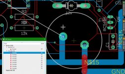
How do I fix this,its mentioned as overlap but the blue layer should be connected to the elyt,how do I do it?
I think the problem here is that it doesn't connect to the pad center but 'overlaps' it. Try to delete that piece of track and re-do from the pad center.
Jan
You´ve to "Ripup" the via not "Delete"!
What Pitch you´ve setting for Autorouter?
I ask you that the Autorouter would not give good results with your Class D Amplifier!
JP
What Pitch you´ve setting for Autorouter?
I ask you that the Autorouter would not give good results with your Class D Amplifier!
JP
Now I have gotten it like it was first -overlap, I have 2 more placec that are like that.
But if I export the gerbers and look at it in a gerberviewer it looks alright .
But if I export the gerbers and look at it in a gerberviewer it looks alright .
If it goes around it and won't connect is because it is not part of the same net. That comes back several times, that has to be fixed.
Does the Help file not discuss the naming of nets?
Or maybe you try to connect two points that are not connected on the schematic.
Jan
Does the Help file not discuss the naming of nets?
Or maybe you try to connect two points that are not connected on the schematic.
Jan
No they are connected in the schamtic.
I cant find anything in the help file except than thet traces can have any name.
I cant find anything in the help file except than thet traces can have any name.
What is the name of the net you try to route? And what is the name of the pad you try to route to? Are they the same?
Jan
Jan
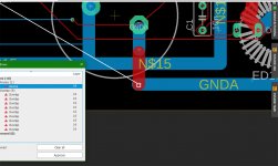
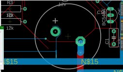
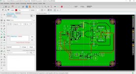
Yes I ripped it upp,but now It won´t let me route to the elyt it just goes around it...
In this picture it is clear you are trying to route to the wrong pad of the capacitor. The N$15 is already connected to the other pad of the capacitor.
This functionality is exactly made to avoid you making a mistake.
Jan
See! Easy.
You need to make a mental switch. You try to force the system to make connections you think are right, and then if the system refuses, you are upset.
If the system refuses to make a connection you think is right, the overwhelming probability is that you are trying to make an error.
You need to understand the concept. The system shows you the correct connections, based on the schematic. Don't fight it.
If you think the system wants to make a wrong connection, go back to the schematic and fix your error.
Jan
Thanks that was fast and fine.I mean wat is the point of making it smaller ....🙂
Beacuse you can...
Beacuse you can...
Smaller, more compact is better as it makes the circuit less susceptible to EMI and other junk. And it takes less space, and cheaper PCB.
But that is the next step, it probably took me 50 or more PCB layouts before I got comfortable with the actual design issues.
Jan
But that is the next step, it probably took me 50 or more PCB layouts before I got comfortable with the actual design issues.
Jan
- Home
- Design & Build
- Equipment & Tools
- Eagle question