I found a way to go back to scrath when doing the autorout.
When I have finnished the schema and the board layout,before doing the autorot.
I copy the Files .sch and .brd to a newfolder. And then I autoroute .And if I wanna go back to before autoroute I just copy the files from the new folder and pase and repalce the routed files.That way i comes back to before autoroute... 🙂
You can double click one the routed wire to reset the wire segment concerned.
Do you guys trust the autorouter?
Do you have correct it some time??
I pick up each track segment that needs to be routed by pressing "q". It finds next shortest segment to route.
If it looks easy I press "g" to autoroute that segment. And fix it if I dont like what it did.
If I want to do it myself then I route it by hand.
This has turned out to be fastest way to route a pcb for me and easiest on the typing.
No not much but I`m learning I have tried Eagle before but not done a finidhed layout with gerber files e.c.t
There are several techniques to doing a layout.
Personally, I already think about the layout when drawing the schematic. Trying to make it as logical as possible, following the signal flow. Power supplies from the top and bottom edges.
Then when I start the layout I normally work from the center of the schematic outwards. For example, if I have a circuit with a couple of opamps, start with one opamp and work towards the end and the start. That usually gives me the most compact and efficient board. Then add the power supply routes on the outside, and the connectors or terminals. Finally draw the board outline.
There are other ways to approach it, but the point is to have a plan, a strategy. Just starting arbitrarily and adding parts randomly will not easily and quickly give you a good, compact layout.
Jan
So I suggest:
- to learn to define missing parts in the managed library (with 3D symbol mapping)
- to draw schematics: I´ll do review
- to start with manual PCB routing: community will review
JP
- to learn to define missing parts in the managed library (with 3D symbol mapping)
- to draw schematics: I´ll do review
- to start with manual PCB routing: community will review
JP
Right now I´m trying to make vias to work,I choose a vias and then choose the other layer and qontinue to route from there Or.
I see sommetime when I delete a line to route it better,but then the lines don´t fit on that same komponent It first was connectet,it refuses to be connected,why?
I see sommetime when I delete a line to route it better,but then the lines don´t fit on that same komponent It first was connectet,it refuses to be connected,why?
Edit: It wont even konnect to the Visas it goes around it or beside it...
Is this som kind of protection kan it be tiurned of?
Is this som kind of protection kan it be tiurned of?
Well if you put in a via and it is not connected to the net you are routing, of course it will refuse to connect, that would be an error.
When you place a via you must assign it to a net if you want to connect to it.
Often the via context menu (right-click) shows you an option to select the net to connect to.
If you want to use a via to switch layers for a track, normally you start the track and when you want to switch layers you do something like a double-click and the system will put in a via and continue to track on the other layer. In Eagle the exact method may be different, Help file is your friend.
Remember, the system wants to help you but foremost avoid any error, because nothing is so frustrating as waiting for a PCB to arrive only to find out that it has errors ... ;-) . With these modern systems, if your schematic is correct, the PCB will also be 100% correct. It will be exactly like the schematic.
Jan
Last edited:
A via must be associated with a net. This can be done inside the schematics: Place a bunch of vias (like a component) and connect these to the nets desired. Then create netlist and import it to NewPCB. Vias are connected to netlist rubberbands now. PCB routing is an Art - and it is the intelligent placement of parts that makes a good design. No automatism can do this for you. Routing after a good placement is easy, autorouters are not the tool for analog circuitry but for complex digital systems loads of parallell data busses.
Last edited:
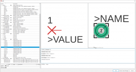
It is not a schematic part, it is a PCB part.
You probably have a list of pads, like SMD, through-hole, edge, and vias.
Try placing a via and right-click, see if there is a selection to select a net. Or check the help file.
Or check how to switch layers while tracking, that will automatically place a via.
Jan
You probably have a list of pads, like SMD, through-hole, edge, and vias.
Try placing a via and right-click, see if there is a selection to select a net. Or check the help file.
Or check how to switch layers while tracking, that will automatically place a via.
Jan
Last edited:
This as far as I get.then I cant move any of them,if right click on the Vias I get the name on it and if I write the name of the wire it asks if I want to connect them toghether. But id doesnt connect them and I cant move them..
CaterpilarSK: Yes Ive thoght about wirepads,but it is the same there that I cannot connect to it the wire goes around it.
Attachments
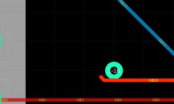
It does show the connection. Probably you can't track from the end of the existing track as it is in a uncommon position. Delete the track then start tracking from the via. Does that work?
Jan
Jan
Last edited:
Yes it works from the via but then it doesn´t connect in the other end..
It's all a matter of net names. Everything you want to connect all needs to have the same net name. Normally it is the case if they are connected in the schematic. Vias are not in the schematic so you must name them manually.
Jan
This as far as I get.then I cant move any of them,if right click on the Vias I get the name on it and if I write the name of the wire it asks if I want to connect them toghether. But id doesnt connect them and I cant move them..
CaterpilarSK: Yes Ive thoght about wirepads,but it is the same there that I cannot connect to it the wire goes around it.
The thing is the wire pads I showed you HAVE TO 100% WORK if you're consistent with the schematic.
If it doesn't then what you do is right click information of the track you want to connect it to (in the PCB) and copy the net name (it's at the total bottom of the window usually named as $XX (xx is some number). You copy that and paste it into the information about the via in the same location where you found it on the track info.
Alternatively you can use the much easier way "net" . Then you just click the desired track and drag the yellow airwire to wherever you want and connect it to whatever you want (if it's a via that you made in the PCB side then you can do that if you actually used the wire pad it won't let you to do so because it considers it a part and doesn't let you do that because you would be inconsistent with the schematic.)
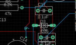
I'll add some pictures for you soon
- Home
- Design & Build
- Equipment & Tools
- Eagle question