how can you make letters appear on the pcb the same way pads do, over the mask? meaning tin plated letters that you can solder.
i thought all you have to do is draw it with 'pad' layer so that the mask doesn't cover over.
please let me know thanks.
i thought all you have to do is draw it with 'pad' layer so that the mask doesn't cover over.
please let me know thanks.
you have to join to layers when producing gerber files. I always recommended to put the text or any kind of other information with special character onto an extra layer to handle it manually
If you open the CAM Processor (blue film icon) and from the file menu, open the job you want, you can see the CAD layers which will be combined into the Gerber layers that go to the board house. For a 2 sided board, the GERBER_RS274X is probably what you want. Tabs appear for each of the output layers you'll get when you process the job. In the 'Silk screen CMP' tab, you'll see which layers are highlighted. All these layers get combined to form the component side silk screen in the default job from Cadsoft. You can add or delete layers (even custom layers) and save the job if you want. I'd keep the Cadsoft job intact and save as. To send the board file out, you'll also need to run an excellon job which creates a drill rack file and a location for all the holes in the board.
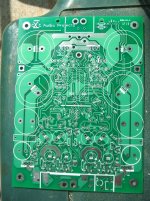
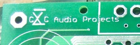
On this PCB, I used top copper layer for the text and then copied the text into the top stop layer and placed on top of the copper layer. This was just a convenient experiment to see if that would work. It did here, but there was a minor problem in using text of different scale. 
I suspect using this method to print text on a specialty PCB would look really good in say, black solder mask color with gold plated copper pads and red silk screen. No need for tinning.🙂😎
I suspect using this method to print text on a specialty PCB would look really good in say, black solder mask color with gold plated copper pads and red silk screen. No need for tinning.🙂😎
Attachments
- Status
- Not open for further replies.