Hey guys,
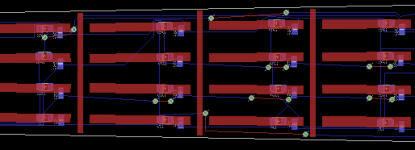
I've designed a two layer PCB with the top layer consisting of rectangles and the bottom layer consisting of some electronic components (i'll include a picture so you can get the idea!), but I have recently realised that rectangles can't be linked to netlists (or if they can, I don't know how!), since i've got quite a few rectangles, could I find some form of script to convert all rectangles to polygons OR could someone possibly suggest a method to connect rectangles to nets?
Cheers,
Harris
Attachments
Rename each rectangle to the same as the net/signal that you want it to connect to (use the info-button in the schematic to find signal names) and then hit the ratsnest-button to refresh.
/U.
/U.
Hey Nisbeth,
Cheers for the reply.
Everytime I try and use the name tool, it just makes that stupid windows 'bing' sound, as if i'm not allowed to do it. Is there another way to name rectangles on Eagle?
Cheers for the reply.
Everytime I try and use the name tool, it just makes that stupid windows 'bing' sound, as if i'm not allowed to do it. Is there another way to name rectangles on Eagle?
Yes, before you draw them. Choose the tool, enter the name of the signal in the command line and press enter. Then draw and it should connect.
/U.
/U.
- Status
- Not open for further replies.