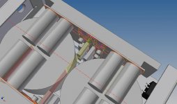
I have 2 toroids 120va 35v (amplimo) which i wanna use to power my ljm 2-12 boards. I don't need the full power of this amp.
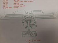
I made a pcb layout with autocad for grinding a pcb.
1 toroid will power 1 amp board.
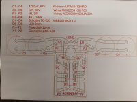
Pcb:
2 fuses (1 per rail)
4 schottky diodes to-220
2 led (1 per rail)
4 capacitors 4700uF 63v. (Nichicon audio grade for the looks)
2 capacitors 1uF with resistor 1R 3W.
Is this design any good for my application?
Should i add or change anything?
I made a pcb layout with autocad for grinding a pcb.
1 toroid will power 1 amp board.
Pcb:
2 fuses (1 per rail)
4 schottky diodes to-220
2 led (1 per rail)
4 capacitors 4700uF 63v. (Nichicon audio grade for the looks)
2 capacitors 1uF with resistor 1R 3W.
Is this design any good for my application?
Should i add or change anything?
Attachments
No, it's not good.From the rectifiers to the capacitors and then from the capacitors to the users.
Not tapping the user connection somewhere in between rectifier and capacitor.
And that goes for positive, negative and ground.
Mona
Not tapping the user connection somewhere in between rectifier and capacitor.
And that goes for positive, negative and ground.
Mona
Oh, is it so much difference with so short connections then?
If i make the circuit, (diode-cap-user), it wil be ok ?
I can't see the difference. Only much longer tracks.
If i make the circuit, (diode-cap-user), it wil be ok ?
I can't see the difference. Only much longer tracks.
Ok, it's no problem to make the circuit like this.
First capacitors and then de load.
The traces will be longer because i can't change the shape of the pcb because of the case it has to fit in..
But i don't see the difference?
Everything is connected with short tracks and a minimum of resistance of these tracks? The caps are still connnected.
Does it make a difference to go first to the cap and then to the load or not. If i do that the traces will be longer.
If you are just making the pcb to show off some expensive capacitors then don't let us stop you, but firstly check which way the writing is on the big caps and orient the pcb pads so you see the writing (rather than it be hidden) !
If you are aiming to reduce hum and noise levels that pass from the rectification process and in to your amplifier then you need to do some homework on power supplies, and electronics, and revisit your pcb design once you have better appreciated what Ketje has posted.
If you are aiming to reduce hum and noise levels that pass from the rectification process and in to your amplifier then you need to do some homework on power supplies, and electronics, and revisit your pcb design once you have better appreciated what Ketje has posted.
I'm here to learn! 🙂
I want a good sounding amp with a good rectifier board.
And i want to make it look good inside the amp.
That's why i want to know what the difference is if to put de caps between the load and rectifier. Or the way i made the pcb.
I can change everything because i haven't ordered anything yet for the rectifier board. 😉
One aspect worth looking at is to snubber the power transformer secondary windings to constrain transient leakage inductance energy to as close to the winding as possible. You may find it worthwhile looking through the Quasimodo threads, and testing your transformer first.
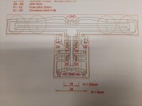
I read a lot of snubbers and add a snubber circuit over the outer taps of the secondairy because there's not much space on the pcb, i learned this should work. I choose the values after measurements.
I also changed the layout of the board. Hope i didn't oversee anything. 😕 🙂
I also changed the layout of the board. Hope i didn't oversee anything. 😕 🙂
Attachments
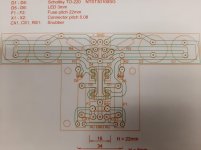
What are R3-C6 and R4-C5 for?
What are CX1 and CS1 and RS1 for?
Perhaps a schematic showing the Tx and secondary windings, and snubber parts, and the pcb and its parts would avoid confusion.
What are CX1 and CS1 and RS1 for?
Perhaps a schematic showing the Tx and secondary windings, and snubber parts, and the pcb and its parts would avoid confusion.
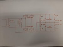
The snubber is usually a C-RC, and is placed across each secondary half-winding, as it is the energy in each half-winding leakage inductance that needs to be constrained.
My fault, the first resistor on the left should be a capacitor. 😱
In the pcb schematic it is a capacitor 🙂
I can try to put a snubber circuit on each half winding. don't know it's gonna fit, but i can try.
I read in different forums that it's no problem to put one snubber circuit over the outer taps, that's why i draw just one. 😕
In the pcb schematic it is a capacitor 🙂
I can try to put a snubber circuit on each half winding. don't know it's gonna fit, but i can try.
I read in different forums that it's no problem to put one snubber circuit over the outer taps, that's why i draw just one. 😕
Check the power dissipated by the current limiting resistors for the LEDs. Don't want to let the smoke out.
It will indeed make it a smokemachine 
The led is rated 20mA 3.2V.
4k7 with 50v will result in 10mA trough the led and near 0.5w in the resistor. I better pick a 0.5w or 1w resistor. Thnx 😉
The led is rated 20mA 3.2V.
4k7 with 50v will result in 10mA trough the led and near 0.5w in the resistor. I better pick a 0.5w or 1w resistor. Thnx 😉
Most new LEDs will happily operate at 2-5mA - perhaps worth checking LED intensity before settling on a resistor dropper value. Perhaps aim for resistor dissipation of no more than 40-50% of rating to avoid brown marks appearing on pcb over the years.
Unless you are very dedicated and have tools available, you won't know if your transformer has a significant level of leakage inductance, or if your power supply configuration is pushing a high level of peak rectifier current and turn-off dI/dt, or if your implementation is leaking rectification noise in to the audio path, and it would have to be a severe case for your ears to pick out any difference.
The snubber is a means of suppressing noise. How well people implement a snubber may be up to practical issues like yours, and once they implement a snubber who knows how they determine if there was a benefit or not ......I read in different forums that it's no problem to put one snubber circuit over the outer taps, that's why i draw just one. 😕
Unless you are very dedicated and have tools available, you won't know if your transformer has a significant level of leakage inductance, or if your power supply configuration is pushing a high level of peak rectifier current and turn-off dI/dt, or if your implementation is leaking rectification noise in to the audio path, and it would have to be a severe case for your ears to pick out any difference.
Thnx for the info,i will try different resistor value's for the led. Maybe 10k, if it's emits light is good enough 🙂
The snubber circuit will be on each half winding, it fits on the pcb.
I will try the quasimodo circuit on the transformer later 😀
Next week i'm gonna mill the pcb, all parts are arrived.
The snubber circuit will be on each half winding, it fits on the pcb.
I will try the quasimodo circuit on the transformer later 😀
Next week i'm gonna mill the pcb, all parts are arrived.
- Home
- Amplifiers
- Power Supplies
- Dual mono PSU.