Following my experiments with the modular power amp https://www.diyaudio.com/community/threads/rcp130-modular-lateral-mosfet-power-amplifier.368795/ where I gathered knowledge regarding several types of input stages I finally chose the mirror loaded complementary symmetrical IPS described here: https://www.diyaudio.com/community/threads/slone-amp-final-solution.379346/
When using a symmetrical complementary IPS loaded with mirrors we face ourselves with the typical problem: “the VAS input voltage is not defined by any reference voltage, so it depends on the VAS base current and the Early voltage of each transistor connected to that node, as well as the common mode offset current of the LTP.”
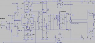
To circumvent this problem, I added a 1k resistor (R12) between the emitters of the top CM (Q10) and VAS bjt (Q3). Fig 1

Fig 1 (R12 action)
According to Keantoken, R12 works actively by converting the VAS and CM into a CCS (analogous to the standard 2Q CCS).
As I see it, the current in the CM is perfectly defined and produces a voltage drop across R2 (Q10 emitter degeneration 133ohm).
R12 transfers this voltage to the emitter of the VAS Q3 so a fixed current runs through its degeneration resistor R11.
NOTE: R12 can not be replicated in the lower VAS (Q5) because that way both positive and negative VAS would try to fix a current in the bias spreader and due to differences in NPN PNP transistors, the current would never be exactly equal… (Both VAS currents would fight each other).
As is, R12 fixes the current on the positive VAS and the negative VAS just follows as if loaded by a CCS.
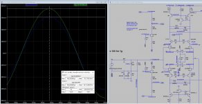
Another benefit from this configuration is that OLG is not severely decreased as in the case where both VAS currents are regulated.
Lowering R12 value increases VAS current stability but lowers OLG. The 1kohm was chosen because it represents a good compromise between current steadiness and High OLG.

Fig 2 (New circuit OLG plot)
-------------------------------------- NOVELTY DRIVEN CASCODE ------------------------------------
I chose to cascode the input jfets because when the cascode is “Driven with output signal” it does minimize voltage fluctuations between the sources and drains of these JFETS.
This “constant voltage” approach can effectively reduce higher order harmonic distortions.
In my prototype, the voltage divider that sets the cascode base voltage Fig 3 (R37 R45) is modulated by input signal through the connection CCSP…. While this method works, there is always a small current diverted from the Jfet sources to the voltage divider and Input Jfets Vds is not really constant.

Fig 3 (Prototype driven cascode circuit)
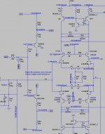
In my new design Fig 4 I chose to drive the cascode bases through a NFB replica coming from the output signal.
In this case the negative feedback replica circuit (R59 R60) modulates both positive (Q7 Q8) and negative (Q12 Q13) cascodes, through the bases of the followers (Q19 Q20).
This way, by carefully choosing R60 value (1k98 ohm) I can stabilize the voltage between the Drains and Sources of the IPS JFETs.

Fig 4 (New Cascode drive circuit)
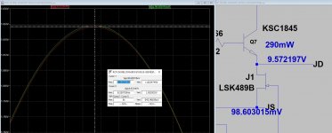
Looking at Fig 5 I placed two test points: JD on the Drain and JS on the source of input jfet J1.
When running the simulation, we see that JD sits at 9.572V and JS at 98.6mV
Plotting V(jd)-9.572 and V(js)-98.6mV we see clearly that both curves are coincident and by tuning R60 we can actually null the difference.
Here we see 542uV Vds voltage variation @ 1KHz 290W.

Fig 5 (Input Jfet Vds plot)
Viewing the results of the .four command Fig 6 (1Khz 290W), we observe that THD is minimized when both curves are coincident.

Fig 6 (1KHz 390W FFT)
I hope this new method gathers enough interest to produce a fruitful discussion on how to best “drive” both cascodes simultaneously.
To facilitate analysis I am including and .ASC file that can be used for testing.
All models are included in the .ASC file so it runs directly in LTSPICE.
This simulation is initially set to produce 300W into a load of 5ohm @ 20KHz
You can choose other values by modifying the values of:
.param power=300
.param freq 20k
.param rload=5
Control transient is:
.tran 0 {{delay}+(20/freq)} {delay} {timestep}
DISCLAIMER:
The present schematic must not be used for commercial purposes.
This is can only to be used as a DIY project.
When using a symmetrical complementary IPS loaded with mirrors we face ourselves with the typical problem: “the VAS input voltage is not defined by any reference voltage, so it depends on the VAS base current and the Early voltage of each transistor connected to that node, as well as the common mode offset current of the LTP.”
To circumvent this problem, I added a 1k resistor (R12) between the emitters of the top CM (Q10) and VAS bjt (Q3). Fig 1
Fig 1 (R12 action)
According to Keantoken, R12 works actively by converting the VAS and CM into a CCS (analogous to the standard 2Q CCS).
As I see it, the current in the CM is perfectly defined and produces a voltage drop across R2 (Q10 emitter degeneration 133ohm).
R12 transfers this voltage to the emitter of the VAS Q3 so a fixed current runs through its degeneration resistor R11.
NOTE: R12 can not be replicated in the lower VAS (Q5) because that way both positive and negative VAS would try to fix a current in the bias spreader and due to differences in NPN PNP transistors, the current would never be exactly equal… (Both VAS currents would fight each other).
As is, R12 fixes the current on the positive VAS and the negative VAS just follows as if loaded by a CCS.
Another benefit from this configuration is that OLG is not severely decreased as in the case where both VAS currents are regulated.
Lowering R12 value increases VAS current stability but lowers OLG. The 1kohm was chosen because it represents a good compromise between current steadiness and High OLG.
Fig 2 (New circuit OLG plot)
-------------------------------------- NOVELTY DRIVEN CASCODE ------------------------------------
I chose to cascode the input jfets because when the cascode is “Driven with output signal” it does minimize voltage fluctuations between the sources and drains of these JFETS.
This “constant voltage” approach can effectively reduce higher order harmonic distortions.
In my prototype, the voltage divider that sets the cascode base voltage Fig 3 (R37 R45) is modulated by input signal through the connection CCSP…. While this method works, there is always a small current diverted from the Jfet sources to the voltage divider and Input Jfets Vds is not really constant.
Fig 3 (Prototype driven cascode circuit)
In my new design Fig 4 I chose to drive the cascode bases through a NFB replica coming from the output signal.
In this case the negative feedback replica circuit (R59 R60) modulates both positive (Q7 Q8) and negative (Q12 Q13) cascodes, through the bases of the followers (Q19 Q20).
This way, by carefully choosing R60 value (1k98 ohm) I can stabilize the voltage between the Drains and Sources of the IPS JFETs.
Fig 4 (New Cascode drive circuit)
Looking at Fig 5 I placed two test points: JD on the Drain and JS on the source of input jfet J1.
When running the simulation, we see that JD sits at 9.572V and JS at 98.6mV
Plotting V(jd)-9.572 and V(js)-98.6mV we see clearly that both curves are coincident and by tuning R60 we can actually null the difference.
Here we see 542uV Vds voltage variation @ 1KHz 290W.
Fig 5 (Input Jfet Vds plot)
Viewing the results of the .four command Fig 6 (1Khz 290W), we observe that THD is minimized when both curves are coincident.
Fig 6 (1KHz 390W FFT)
I hope this new method gathers enough interest to produce a fruitful discussion on how to best “drive” both cascodes simultaneously.
To facilitate analysis I am including and .ASC file that can be used for testing.
All models are included in the .ASC file so it runs directly in LTSPICE.
This simulation is initially set to produce 300W into a load of 5ohm @ 20KHz
You can choose other values by modifying the values of:
.param power=300
.param freq 20k
.param rload=5
Control transient is:
.tran 0 {{delay}+(20/freq)} {delay} {timestep}
DISCLAIMER:
The present schematic must not be used for commercial purposes.
This is can only to be used as a DIY project.
Attachments
Last edited:

The new Driven Cascode circuit for complementary differential symmetrical input stages Fig 4
Please note that Net Labels +15V and -15V are just labels... in reality the cascode bases are not biased at +-15V (I am using +-10V for the cascode bases)
Please note that Net Labels +15V and -15V are just labels... in reality the cascode bases are not biased at +-15V (I am using +-10V for the cascode bases)
Attachments
R12 compromises CM operation, that is 1:1 relation of two sides.
Cascode driven by nfb voltage will lag behind input voltage and can't provide stabile Vds of input jfets.
Cascode driven by nfb voltage will lag behind input voltage and can't provide stabile Vds of input jfets.
Dear chip_mk
Thank you for your comment.
In fact I am following Bob Cordell's advice published in Linear Systems LSK389 app notes and it does work very well in another of my builds.
If you run my sim, you will find that input jfets VDS is effectively frozen with this method... please look at fig5
Thank you for your comment.
In fact I am following Bob Cordell's advice published in Linear Systems LSK389 app notes and it does work very well in another of my builds.
If you run my sim, you will find that input jfets VDS is effectively frozen with this method... please look at fig5
Attachments
Dear Ricardo,
very interesting design. Waiting for your first prototype. Will have a deeper look into your design.
👍😉
very interesting design. Waiting for your first prototype. Will have a deeper look into your design.
👍😉
Thank you astxDear Ricardo,
very interesting design. Waiting for your first prototype. Will have a deeper look into your design.
👍😉
I am allready designing the pcb... Will post it here soon
Dear Ricardo,Dear chip_mk
Thank you for your comment.
In fact I am following Bob Cordell's advice published in Linear Systems LSK389 app notes and it does work very well in another of my builds.
If you run my sim, you will find that input jfets VDS is effectively frozen with this method... please look at fig5
I'd prefer bootstraping like 5b for simplicity and speed. Anyway, the amp might end up performing very well inspite concerns I've mentioned.
P.S. How does Vds of the input jfets look like in your simmulation for square input signal?
Indeed bootstrapping with a follower does provide very good results and it is also my prefered option.... but in this case I did not find a way to reduce Vds variations below 100mv.Dear Ricardo,
I'd prefer bootstraping like 5b for simplicity and speed. Anyway, the amp might end up performing very well inspite concerns I've mentioned.
P.S. How does Vds of the input jfets look like in your simmulation for square input signal?
Driven from the output it is possible to reduce Vds variations below 1mV .....
The downside is that there is always that small phaseshift between the signal on cascode bases and jfet sources...
How about bootstrapping with a follower plus a current source in follower's source? Wouldn't it reduce Vds variations enough and make cascode voltage more insensitive to supply voltage variations than 5c?
I will try it....How about bootstrapping with a follower plus a current source in follower's source? Wouldn't it reduce Vds variations enough and make cascode voltage more insensitive to supply voltage variations than 5c?
But I believe that to reduce vds variations we need to be able to control the level of the signal injected in the cascode bases.....
Using Jfet followers to bootstrap cascode base voltages to the input signal eliminates the phase shift between VD and VS in the input jfets.
In this case VDS variation in the input jfets is near 135mV... (much larger than with my initial circuit) but maybe eliminating the phase shift is more important in this case.
I am using LSK170 / LSJ74 for simulation as I did not find any better alternative.
R59 and R60 20kohm resistors needed to lower VDS in these followers.
I did not notice any improvements by replacing R83 and R84 (33kohm) by a ccs.
Attachments
Crucial to minimize Vds variations is to replace R45 and R49 with zeners, I think 10V (alternatively just bypass them with 47uF elco).
For additional improvements you can consider using current source, reduce R10 and R47 to 100ohm, bypass R59 and R60 with 100nF, and use 2SK245 and 2SJ103 as followers.
For additional improvements you can consider using current source, reduce R10 and R47 to 100ohm, bypass R59 and R60 with 100nF, and use 2SK245 and 2SJ103 as followers.
The zener with the bypass cap reduces VDS variations to 2.5mV and there is no phase shift visible @ 20khz.... very good.
Can not find 2SK245 / 2SJ103 do you know a source ?
Can not find 2SK245 / 2SJ103 do you know a source ?
It was a mistake... I have corrected the post now.Can you bit explain about this early slew, what does it mean?
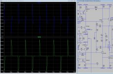
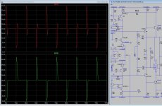
What I am struggling with is an abnormal spike appearing on the positive VAS collector current.
This spike is not present in the negative VAS.
This can be seen only with 50khz square wave test.
It is worst with small signal (0,1v) in the input.
With higher input voltage (0,8v) it looks like overshoot.
- Home
- Amplifiers
- Solid State
- Driven Cascode Novelty Circuit