i've been reading Doug Self's book, as well as Randy Slone's book. i always thought that double diff amps were somewhat redundant, but i modeled Slone's input stage test circuits in LTSpice, using 2N3904 and 2907 transistors, and i like the results. i'm thinking of building a kind of "universal op amp" using something like the double diff amp that Slone's book shows. in fact, it will have differential inputs, +/- side comp cap pins, and +/- vas outputs. the idea is to build a bunch of these modules, and use them with whatever output stage combination that suits the application. it would even be feasible to use them as a high voltage op amp by themselves. the thing i like (that never before ocurred to me) about this topography is the symmetrical slew performance. the fact that the offset currents cancel is a good feature as well.
The SWTPC 198B preamp had four such 3"x3" modules in it.
Picture of the earlier version (looks the same, but single-ended diff pair).
I used to buy these used to gut and steal the modules out of.
The stock supply in the complete preamp wasn't very good, but with an external supply this was a hard piece to beat.
Picture of the earlier version (looks the same, but single-ended diff pair).
An externally hosted image should be here but it was not working when we last tested it.
I used to buy these used to gut and steal the modules out of.
The stock supply in the complete preamp wasn't very good, but with an external supply this was a hard piece to beat.
Hi
Are you referring to figure 4.10a on page 94 of this book?
http://books.google.com/books?id=LoXH1YkyhUUC&pg=PA73&lpg=PA73&dq=slone
Are you referring to figure 4.10a on page 94 of this book?
http://books.google.com/books?id=LoXH1YkyhUUC&pg=PA73&lpg=PA73&dq=slone
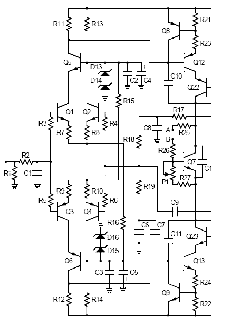
that's the test circuit. the actual discrete op amp i'm going to make and use is a bit different, but based on the test circuit. it will be a module. depending on how it is connected, it can be a high voltage op amp, or input/VAS for a power amp. i think the trick will be choosing the right transistors. depending on what it is used for, some of the transistors will need to be a bit beefier than the 2N2222/ 2907 models i used in LTSpice. i suppose for an op amp type application 2N2222/2907's would work, but in a power amp, the VAS transistors would have to be higher voltage and current devices. i tried adding bipolar outputs (MJW0281,MJW0301 IIRC) and the model at least tested out at .001% THD at full output 1khz, and .003% THD at 20khz.
test circuits and models are one thing, but using real silicon is another, since there are things that models don't test for, such as magnetic coupling of the power supply wiring to the input stage, etc, which can cause distortion and noise. although, i would be happy with the first prototype doing as well as .01% THD, and i can play with the circuits to get closer to .001%. some classic amps actually had to have the wiring moved around to null out the distortion caused by power supply rail magnetic effects. one trick will be to get the input stage real estate down to the smallest size possible. actually models can test for such things if you treat every component lead as a weakly coupled inductor, but you can't move wires around on a model.....
since the offset currents come pretty close to cancelling between the NPN and PNP inputs, there isn't much DC offset, even without some type of DC correction (such as a cap in the feedback loop or a DC servo). the model measured 25mV offset at the output with an Av of 20.
Hi Uncle
If you aren't afraid of more parts, cascode(s) might come in somewhere here. I have found that using a cascode VAS is quite nice too.🙂 The drawback is that you will loose a few volts, so a higher voltage supply is needed, relatively small current of course. If you use a Mosfet source follower output stage, you will need a higher drive supply anyway. The advantage is that you can keep a constant Vce on the amplifying transistors as well as being able to use much lower Vce small signal, fast, low noise, low Cob devices. The larger, higher Vce cascode transistor will then be driven as a common base instead of common emitter. There may be a small advantage in this.
Have you ever simulated a cascode double differential, driving a cascode double differential VAS circuit?😀
"Have you ever simulated a cascode double differential, driving a cascode double differential VAS circuit?"
No, but it sounds pretty good on speakers.
No, but it sounds pretty good on speakers.
i am pretty sure i'm going with the stabilized beta BJT's for the outputs. my preliminary design uses the VAS as drivers, but this does some squirrely things with the bias transistor (it's difficult to get a transistor to operate reliably at 1.4V C-E), so i'll add a set of drivers, just to get the bias circuit to work correctly. i'll see what happens if i cascode the VAS as well, but the darlington VAS in slone's book looks interesting as well. the complete input stage/VAS will be a potted module, which should give good thermal tracking in the diff amp. it will also simplify circuit board design of any amps i build, since the only layout to consider wil be the driver/output stage. i'm going to use SOA detection and relay for overload protection rather than the usual VI limiter for two reasons.... first a cycling relay is a sure indication of problems with the load, second with marginal loads, the VI limiters have a tendency to "predistort" the output stage, but the operation of a SOA detector doesn't effect the output waveform at all.
- Status
- Not open for further replies.
- Home
- Amplifiers
- Solid State
- double diff amps