Guys this is the psu segment of my modular preamp. To the left would be the pcb mounted trafo and from that ac shunt> double bridge rectifier> lm317/337 regs> darlington cap mx then to the preamp modules which are not drawn. I tried to be meticulous with the star grounding but as you can see i have no formal training with this work and would like your help in determining if my layout is violating any must-follow rules. Thank you in advance.

I think the - return traces from the big filter cap to the rectifier should be as short and thick as possible, they carry the big charging current spikes. These currents should be kept away from the central star ground to avoid hum issues. In the current trace routing, the cap recharge pulses take the long way from the cap to the central star and back to the rectifier. Any voltage differential over that path changes the potential of the star ground point, possibly leading to hum.
Regards,
Rundmaus
Regards,
Rundmaus

Trying again for higher rez upload
An externally hosted image should be here but it was not working when we last tested it.
I think the - return traces from the big filter cap to the rectifier should be as short and thick as possible, they carry the big charging current spikes. These currents should be kept away from the central star ground to avoid hum issues. In the current trace routing, the cap recharge pulses take the long way from the cap to the central star and back to the rectifier. Any voltage differential over that path changes the potential of the star ground point, possibly leading to hum.
Regards,
Rundmaus
Thank you Runemaus. So a thick continual trace from the rectifier to - pin of the cap then to the star ground?
Does it have any benefit to keep the tracks from each diode seperate until they meet at the cap?
And if the rectifiers are the ultimate return point shouldnt i shift my star ground toward them?
Last edited by a moderator:
It would probably be better replacing the octopus ground with a ground plane. Try to reduce loop area to a minimum and strategically place the parts so as not to overlap the loops.
Star ground for everything is not a good approach. Certainly the transformer/diodes/main filter capacitor
should be arranged as a local group, to avoid current charging pulses coupling into other circuit branches.
Then the two filter capacitor nodes are brought out from that subcircuit for connection. Or a ground plane
will work well with reasonable component placement. It can be a good idea to keep the two secondary windings
and power supplies isolated, only connecting their commons together at the output terminals.
Last edited:

a power supply should flow through.
rectifier, smoothing caps then out to rest of circuit.
smoothing cap charging current impulses can cause havoc with audio signals.
rectifier, smoothing caps then out to rest of circuit.
smoothing cap charging current impulses can cause havoc with audio signals.
Does this look better, guys?

Or should i combine L and R tracks for the main psu caps, essentially closing the slit beteen them?
Or should i combine L and R tracks for the main psu caps, essentially closing the slit beteen them?
I usually divide the plus and minus sides to their own side of a board.
Main ground running straight down the middle.
Never had any hum issues yet.
Main ground running straight down the middle.
Never had any hum issues yet.
I'd put plus and minus on their own side and a ground plane on the bottom.
The octopus ground will make your ground issues worse, not better, as it maximizes the ground impedance. A plane is the lowest impedance you can get.
Tom
The octopus ground will make your ground issues worse, not better, as it maximizes the ground impedance. A plane is the lowest impedance you can get.
Tom
Hi donovas,
A few comments ...
... And then may I suggest looking at where the currents flow in and out between the various components and ground?
If a ground plane is used this will typically give an overall lowest impedance, however, it may be feasible to make sure that the currents of the various parts of the PSU do not interfere with eachother (also not in the ground plane). This can be visualized by maybe drawing up where the currents go in and out of the components and toward the ground (plane).
When that is reasonably clear I would assume that the above suggestions - and a feasible spacing between the components - are good starting points.
Cheers,
Jesper
A few comments ...
+1a power supply should flow through.
+1a ground plane will work well with reasonable component placement.
+1I usually divide the plus and minus sides to their own side of a board.
Main ground running straight down the middle.
... And then may I suggest looking at where the currents flow in and out between the various components and ground?
If a ground plane is used this will typically give an overall lowest impedance, however, it may be feasible to make sure that the currents of the various parts of the PSU do not interfere with eachother (also not in the ground plane). This can be visualized by maybe drawing up where the currents go in and out of the components and toward the ground (plane).
When that is reasonably clear I would assume that the above suggestions - and a feasible spacing between the components - are good starting points.
Cheers,
Jesper
Thank you everyone for their knowledge. Im sorry but i dont quite understand what you mean by separate plus and minus. Do you mean the ground layer of each psu polarity? If im to keep them seperate then where should i join the signal ground?
Heres an alternative layout i did since last night. Please let me know if this is better
Heres an alternative layout i did since last night. Please let me know if this is better
An externally hosted image should be here but it was not working when we last tested it.
At first glance that's looking a lot better, can you post a schematic? Join the grounds right at the output
Thank you, Scott. It looks like the schematic is indicating that the join location should be at the 1st smoothing cap?
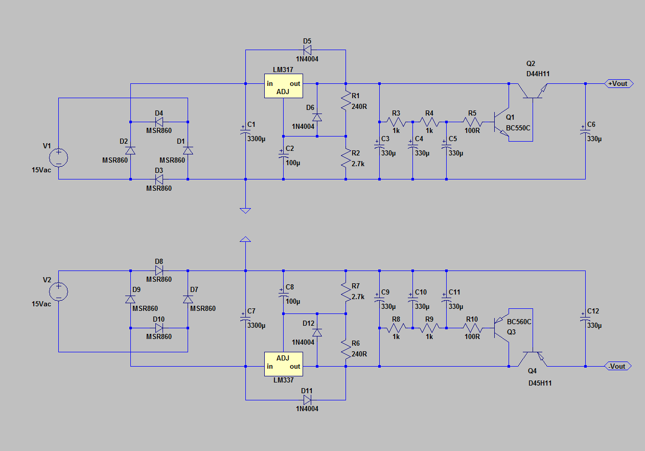
The schematic is from F5-HA thread, btw
The schematic is from F5-HA thread, btw
It probably wouldn't make much difference so long as you don't take the output from there but then there's no need to separate them down the middle of the board. It's all about trying not to create any potential loop, however small. If it's connected both ends technically it's not a loop just two parallel paths as nothing should be able to flow around it.
I'd ask the mods to shift this thread to "power supplies" if I were you
I'd ask the mods to shift this thread to "power supplies" if I were you
Last edited:
That 2nd layout is a LOT better.
But I have a comment on the circuit.
You should put the cap multiplier first, and the regulator 2nd. The way it is now a lot of the good performance of the regulator is negated by the cap multiplier.
The cap mux should come first to squash the ripple and mains junk, then the regulator to provide rock-stable and noise free, low impedance DC.
Jan
Jan, the circuit was used by john curl in his earlier preamps. Its my understanding that the darlington cmx will have lower noise and lower output impedance than the lm317 so it makes sense to put it downstream?
@donovas:
IMHO there's one more thing to the sequence of the regulator and the capacitance multiplier: The LM317 is a device with feedback so there may be some "ringing" in its regulation.
The capacitance multiplier is a "passive" configuration - just "keeping the voltage" it sees on the base of the first transistor (minus some slightly variable base-emitter voltage drops).
If it were me I would stay with the sequence as is (and it is my opinion here ;-)) yet I would add a current increasing resistor to the emitters of the BC550 and BC560. This will increase the bandwidth of these transistors, however, in my experience they very likely will sound somewhat better as well. A suggestion could be a resistor that gives a 5 mA current.
To my knowledge the output impedance of the DH4* will depend on the current drawn (appr. 26 ohms for 1 mA; ~5.2ohms for 5 mA, etc.) but others may have more input here. This also means that depending on the current draw in your actual circuit the LM317/337 may have a lower output impedance if that is important to you.
Cheers,
Jesper
- Home
- Design & Build
- Software Tools
- Does my layout look ok?