Hi,
i was searching through net information about DNM 3A.
I got second hand, but without PSU. I complain, but for now without success.
I contact DNM, they give poor info about output voltages +-30V DC. I suspect they are not correct as capacitors are 25V rated.
Could you please share your PSU solution to me?
At least i will be happy with voltages and pins position (first and last pins are +-) 😀
Best regards, Bostjan from Slovenia
First step would be to look at where the power pins go internally.
What are the first components they come to?
Are there any voltage regulators in there?
Do the power pins connect directly to any of the caps that are marked 25V. In other words are any of those caps across the incoming supply?
If so then that sets an obvious upper limit.
My first guess would be this runs on around -/+15 to 18 volts DC as that is a fairly common value.
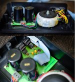
Well that transformer appears to be 36VA, 24V+24V 0.75A, into some regulator ICs, which means about +/-32V unregulated, perhaps +/-28 or 24V regulated? 24V sounds more likely given the caps, and there are standard regulator chips for 24V too.
Last edited:
DNM 3A preamplifier
Hi guys, thanks for reply.
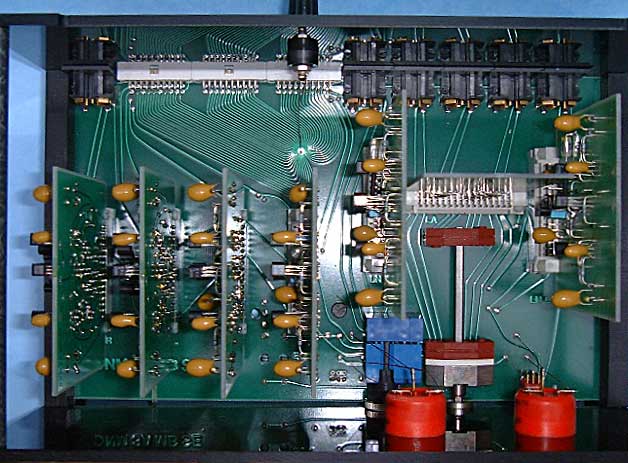
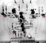
There is no voltage regulators in preamplifier. There are in PSU unit as photo above TVI send.
I follow pins from PSU connector, it goes separately to left and right channel and every board.
On small board goes direct to transistors. All transistors are erased markings, so i dont now what they are.
My attempt is not to reveal manufactor design only proper connection of PSU.
Anyway i will post small boards phots from both side, so you can see where voltages came to board.
Only i can do, i could put transistor, one by one and with arduino tester see condition and type of transistor.
Well that transformer appears to be 36VA, 24V+24V 0.75A, into some regulator ICs, which means about +/-32V unregulated, perhaps +/-28 or 24V regulated? 24V sounds more likely given the caps, and there are standard regulator chips for 24V too.
Hi guys, thanks for reply.
There is no voltage regulators in preamplifier. There are in PSU unit as photo above TVI send.
I follow pins from PSU connector, it goes separately to left and right channel and every board.
On small board goes direct to transistors. All transistors are erased markings, so i dont now what they are.
My attempt is not to reveal manufactor design only proper connection of PSU.
Anyway i will post small boards phots from both side, so you can see where voltages came to board.
Only i can do, i could put transistor, one by one and with arduino tester see condition and type of transistor.

It is very difficult to say with any certainty.
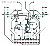
At the top of the board are what look like zener diodes, and they could be part of a local regulator on each board.
What do the markings say on these two parts?
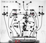
This 2 parts marking: C10 811 Motorola
Boards has tantalum capacitors, so have to show polarity:
Attachments
Most likely a 10V zener.
I think what you need to do is to power this up on preferably a variable split supply or failing that a supply of say -/+15 volts and then measure the voltage across all the tants.
See if any of those caps see the full supply or very near to it.
If they do then that sets an absolute limit of -/+25 volts and so in practice means the unit most likely ran on -/+18 as a maximum.
If the emitter of the transistors near the zener have around -/+ 9.5 volts on them then they may be local regulators in which case the unit may run on a supply nearer -/+15 volts.
If you make or buy a supply using 78 and 79 regs or adjustable regs like the LM317 then you can work up in voltage and see at what point circuit conditions stabilise.
DNM are practically undocumented on the web. It will certainly be worthwhile to draw an approximate circuit from the pics. For this it would be great to see the component side in colour and have the transistor polarities marked. If not too much trouble 🙂
DNM are practically undocumented on the web. It will certainly be worthwhile to draw an approximate circuit from the pics. For this it would be great to see the component side in colour and have the transistor polarities marked. If not too much trouble 🙂
OK, i will do. It will take some time.
Since i was impatient, i tried connect with +-25V DC, makes some tantal capacitors smoking.
I will of course change them, and tried all transistors with arduino tester, to see if they are good, type, so it will be easier to make schematics.
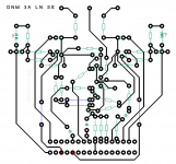
Well the bottom two transistors form an NPN differential pair, and the one above it (PNP) is driven from this and has feedback network to the pair. Above that are two transistors in some sort of emitter follower configuration, NPN.
Its made harder to understand and many signals go off-board or come from off board.
At the top are I think shunt regulators for the rails. The three connections at the top are possibly outputs, or maybe rails in and output signal. I think all the transistors are standard ECB TO92 pinout. Its not clear where ground comes into the board but I think the two top capacitors lead to ground pins on the connector.
Last edited by a moderator:
Shunt or series...
I think the regs are classic series types with a Zener reference on the base of the series pass element.
I think the regs are classic series types with a Zener reference on the base of the series pass element.
Does this help?
wow, nice and clear
busy this weekend to much.
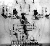
But before sleep i make more markings:
Attachments
Well the bottom two transistors form an NPN differential pair, and the one above it (PNP) is driven from this and has feedback network to the pair. Above that are two transistors in some sort of emitter follower configuration, NPN.
Its made harder to understand and many signals go off-board or come from off board.
At the top are I think shunt regulators for the rails. The three connections at the top are possibly outputs, or maybe rails in and output signal. I think all the transistors are standard ECB TO92 pinout. Its not clear where ground comes into the board but I think the two top capacitors lead to ground pins on the connector.
later i will check more connections where it goes (GND, ...)
it has star ground connections every where, probably to reduce ground loops.
- Home
- Source & Line
- Analog Line Level
- DNM3a primus amplifier PSU