We need a list of transistors and diodes that Scott modeled with other than the j111. Did he use the latest Hitachi/Toshiba transistors and what are the output devices. The schematic is no longer mirror symetrical. Granted I'm not an EE and i trust Scott's design.I was told by another Phd EE that the 2n4403/2n4401 transistors have low base spreading resistance, the 03 particularly. Are there more modern transistor/s that are better. I will wait before starting to layout my board. It's too up in the air. Ray
At their locations in SW's circuit, low rbb' is not that critical.We need a list of transistors and diodes that Scott modeled with other than the j111. Did he use the latest Hitachi/Toshiba transistors and what are the output devices. The schematic is no longer mirror symetrical. Granted I'm not an EE and i trust Scott's design.I was told by another Phd EE that the 2n4403/2n4401 transistors have low base spreading resistance, the 03 particularly. Are there more modern transistor/s that are better. I will wait before starting to layout my board. It's too up in the air. Ray
Some very good parts that have high betas and breakdown voltages: 2SA970, 2SC2240, BL beta codes preferred. Although Toshiba does not mention rbb' explicitly for them, I backed out an estimate of 30 ohms for the 970, which is as good or better than the 4403. The low rbb' of the 4403, a fortuitous consequence of Motorola's trying to make a better switch, was a trade secret in places for a while. But that was long ago 😀 BTW not all 4403s are the same.
The output devices on the other hand I'm not as sure about. The input JFETs I believe are BF862 if you have the patience to deal with SMD and to match them.
Should I use this for PCB layout ?
Patrick
I'll need one more post to show where some small R's and C's can go to help with lower closed loop gain applications. The input clamp diodes (back-to-back on the input like on the JE990 and many IC's) are also needed.
I have been using the Toshiba devices for the latest sims but the others will work. The bipolars figure very little into the noise budget, just trying to get the higher rails.
I hope someone will tinker with a breadboard, I don't trust the sims at the finest scale especially getting it unity gain stable.
It may be worth while to look at output protection as well. With a shorted output the sim suggests well more current than needed to slag any small signal output transistors.
Dave
Dave
It may be worth while to look at output protection as well. With a shorted output the sim suggests well more current than needed to slag any small signal output transistors.
Dave
Live dangerously for the best sound.😀
As the whole left hand corner is now just 'constant current source' stuff, can't we get rid of J1, Q11, 9 and tie the bases of Q15, 35 to emitter & collector of Q7 respectively?Latest schematic, I added input cascodes and tied the bias setting current surces together at the drains so only one cascode would be needed (for operation at high supply voltages).
Live dangerously for the best sound.😀
I keep hearing that. Something about fearless... I tend to side with Stapp. 🙂
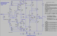
If you are using a discrete op-amp it's crazy not to take advantage of the ability to custom compensate it for each application. After an afternoon's work it looks like the compensation capacitance needs to be circa 250pF at unity gain and can be as low as 75pF for 20dB of gain. Now even the first circuit has 50V/usec symmetrical slewrate at 20dB gain. I suggest here components that can be adjusted to optimize frequency response and assure stability. I realize that the details of optimizing this circuit are beyond the abilities of some of the folks here so let's help each other and include placeholders for the optional components in any layout and those that can develop a parts list for a specific application can inform the rest of us.
I have added a zero in series with the compensation capacitance as well as a pole zero network in both sides of the gain stage. These values depend on closed loop gain and matter less at G > 10.
EUVL - I consider that there is enough here to burn a prototype.
I have added a zero in series with the compensation capacitance as well as a pole zero network in both sides of the gain stage. These values depend on closed loop gain and matter less at G > 10.
EUVL - I consider that there is enough here to burn a prototype.
Attachments
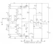
As the whole left hand corner is now just 'constant current source' stuff, can't we get rid of J1, Q11, 9 and tie the bases of Q15, 35 to emitter & collector of Q7 respectively?
Yes that could be, as long as the dynamic base current is captured it all works, time to Muntz away a little.
EDIT - It does not work out that easily, best left alone for now.
Last edited:
To keep the ball rolling, here's a quickie knock up of the schematic from #1568 for those who are averse to fiddling with the versions already posted. Appears to be OK, haven't checked everything, I'm sure people will point to any problems ... 🙂
The PSRR looks much, much better of course. One thing though, can't push the output standing current up to 8mA easily for some reason ...
Frank
The PSRR looks much, much better of course. One thing though, can't push the output standing current up to 8mA easily for some reason ...
Frank
Attachments
To keep the ball rolling, here's a quickie knock up of the schematic from #1568 for those who are averse to fiddling with the versions already posted. Appears to be OK, haven't checked everything, I'm sure people will point to any problems ... 🙂
The PSRR looks much, much better of course. One thing though, can't push the output standing current up to 8mA easily for some reason ...
Frank
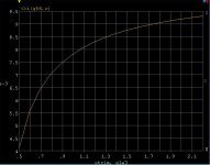
Fiddle around with R10 vand R11, make them a little bigger and then do the trim. There certainly are values that get the desired currents.
> EUVL - I consider that there is enough here to burn a prototype.%
Noted.
Am busy the next week or so, so it will take a while.
Patrick
Noted.
Am busy the next week or so, so it will take a while.
Patrick
Last edited:
Yes, simple adjustment of R10=R11= 30R will do it. Then values of R18 from 540 to 640R depending on the BJTs get it there.Fiddle around with R10 vand R11, make them a little bigger and then do the trim. There certainly are values that get the desired currents.
Which would you suggest as the best way for trimming the DC operating point?
Frank
Are transistors Q15 and Q16 thermally coupled to the output transistors Q11 and Q14? Should R18 be a ten turn? Is it gona be tweaky if not a ten turn? Thanks, Ray
Should there be anti latch up diodes on the input(1n6263)??? Thanks, Ray
I would use ordinary diodes, plenty of SMT duals out there like BAV99/199 for instance. I use the 99's for normal clamp use and the 199 has <200fA typical leakage if needed.
Here's a plot of the trim, looks like a 2k pot would be better once the small resistors are picked. Depending on the devices I would pick R10 and 11 to max the bias out at 10ma or so then the trim always goes down to the desired value. You could also just select R10 and 11 to get around the right value the absolute Vbe's won't vary that much.
Checked over supply and temp should be no problems with simple thermal contact between the four output devices.
Attachments
Last edited:
Here's a JFET JE990 with up to date parts. The J305 is a place holder since I did not have models for the depletion mode MOSFET's. These devices would also do a nice PA front end. I can't offer much help since this is LTSPICE, but it looks like a nice project.
Thanks to Pete Basel for entering the original.
Thanks to Pete Basel for entering the original.
Attachments
Last edited:
Here's a JFET JE990 with up to date parts. The J305 is a place holder since I did not have models for the depletion mode MOSFET's. These devices would also do a nice PA front end. I can't offer much help since this is LTSPICE, but it looks like a nice project.
Thanks to Pete Basel for entering the original.
Hi Scot,
Thank you.
What depletion mode MOSFET's would suit here?
Hi Scot,
Thank you.
What depletion mode MOSFET's would suit here?
The C. P. Clare devices like the CPC3730 are very attractive. There are 4 makers now with promising devices and it seems there are enough conventional applications that they will remain available.
The J111 will work too.
EDIT - Just a note we are enjoined from installing LTSPICE on computers owned by our company, this is perfectly within reason since they are paying the bills.
Last edited:
Scott I assume you meant the 2nd definition re: LTspice?
tr.v. en·joined, en·join·ing, en·joins
1. To direct or impose with authority and emphasis.
2. To prohibit or forbid.
jan
tr.v. en·joined, en·join·ing, en·joins
1. To direct or impose with authority and emphasis.
2. To prohibit or forbid.
jan
- Home
- Source & Line
- Analog Line Level
- Discrete Opamp Open Design